
In this paper, a large-scale . RLC filter is proposed with the aim to suppress common mode (CM) noise that takes place within parallel conducting plates in high power systems. For this purpose, the filter model was created in COMSOL Multiphysics 6.0, run Maxwell’s equation for electric field in frequency domain, and evaluated with good results in derived equations for CM transmission coefficients using CISPR 17 methods. The proposed structure with shielding enhanced the simulations CM noise (< - 25 dB) within the range of 1 MHz to 220 MHz. As an application, variations in phase (0°-180°) and amplitude device output obtained along frequency.
Index Terms – Electromagnetic Compatibility (EMC), Common Mode (CM), Power systems, Simulations, RLC Filters
I. Introduction
Many research efforts have been indicated that the fast-switching behavior (high dv/dt and high di/dt) of semiconductor devices might cause electromagnetic noise radiated EMI and surge voltage [1]- [5]. Radiated EMI can be suppressed by reducing the common mode (CM) currents flowing from an excitation source [6]-[8]. In addition, the stray-inductance and -capacitance are also one of most important factors for the surge voltage. Several planar busbar designs have been presented in the literature for different applications [9]-[20]. For each bus bar type a suitable model to aid a designer was developed. Inductors are important design consideration when it comes to high power applications because they offer low losses, high frequency and provide a reduction of saturation magnetic flux density due to temperature increase of their core [21]-[28]. This circuit component contributes weight, volume, and magnetic materials in core.
The attractiveness of using devices such as fast RF ferrite phase and amplitude modulators that control the magnetic states of the ferrite is widely recognized [29]-[32]. Big rough objects physically spread out and it will affect how it behaves at high frequencies. Because there are large physical dimensions to the object here and it is insufficient to simulate in Spice (Simulation Program with Integrated Circuit Emphasis). The article is organized in the following sections,
I. Introduction.
II. Design, build and optimize the device in COMSOL Multiphysics 6.0. Material selection for components and structural optimization. Electromagnetic shielding is essential to the device. A current generating circuit is presented in LTspice.
III. Employing CISPR 17 methods to determine the CM transmission coefficients and thereafter estimate amplitude difference and phase difference at outputs. Maxwell’s equations for electric field are presented at the end of the section.
IV: The electric field distribution is determined to verify the effectiveness of the proposed model.
II. Filter Design
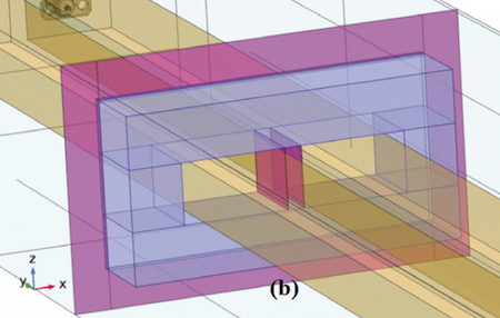
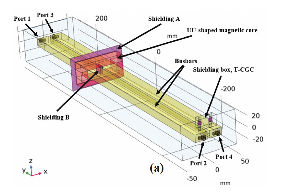
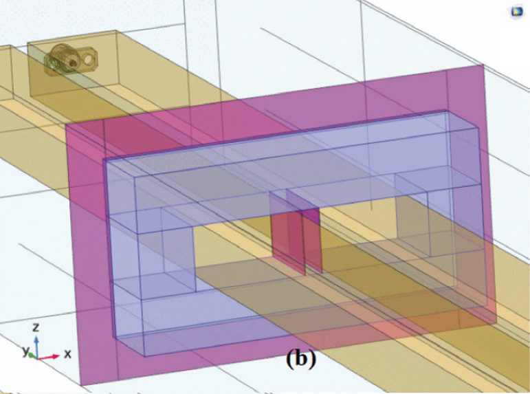
A 4-port simulation model including a RLC filter is created in COMSOL, as shown in Fig. 1. The filter consists of two busbars, a UU-shaped magnetic core, and two capacitors encased in a grounded shielding box such that the capacitors are coupled in series with their common connection connected via metallic sheets to the box forming a tailored capacitor-ground-capacitor (T-CGC with capacitors described in subsection E, see also Fig. 5). The capacitors are connected to the busbars via metallic sheets. The T-CGC is placed in the grounded shielding box to offer protection from any EM interference. The UU-shaped magnetic core is joined by shielding A and shielding B (Fig. 1(a) and 1(b), see also subsection B). The filter is placed in a 4-port simulation box model (section III, subsection A, a 4-port simulation model) to meet CISPR demands [15]. The busbars are coupled by a parallel RLC circuit that has a characteristics RLC (Fig. 1(c), see also subsection F, 1 Ω, 14.61 uH, 85.15 pF). The UU-shaped magnetic core is positioned 400 mm from the shielding T-CGC box. The size of a busbar is 518.4 mm x 22.3 mm x 13 mm (subsection C). The shieldings are grounded condcutive.
A. LTSpice circuit design
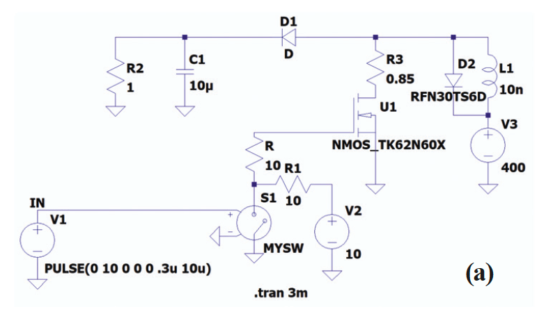
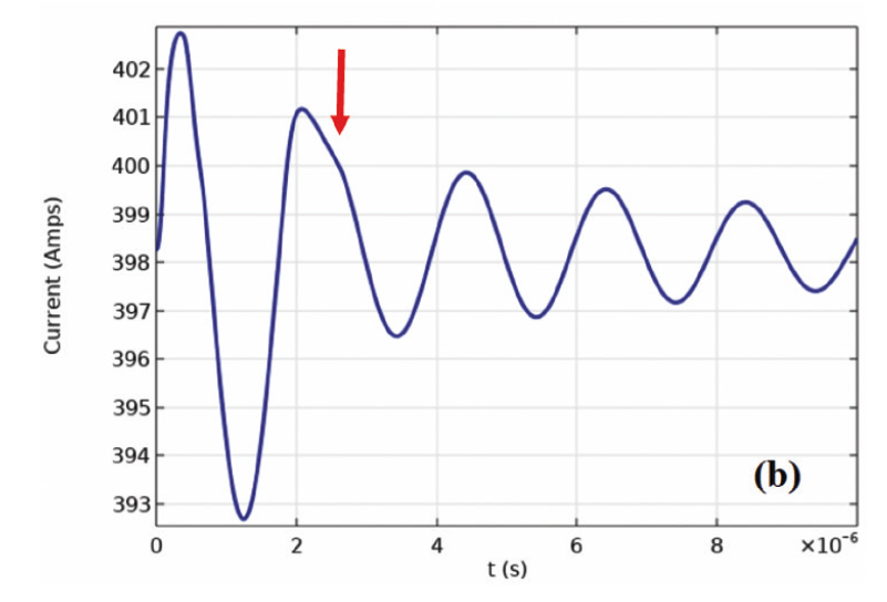
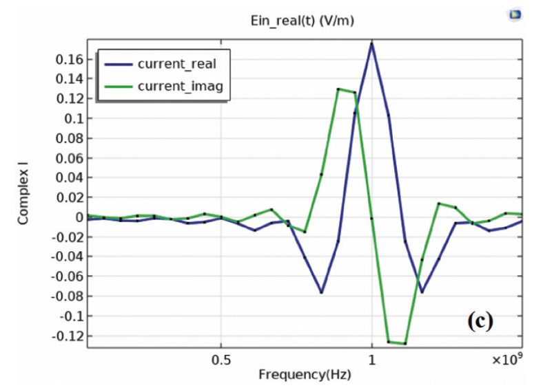
Fig. 2 (a) shows a switch-controlled boost converter designed to verify the performance of the device. It is shown that the circuit exhibits spike behavior (Fig. 2(b)). The NMOS turn-off voltage spike is affected by not only the inductance L1 but also the diode forward recovery characteristics D2 under high voltage high current conditions. An oscillatory behavior of the persistent avalanche current can be distinguished due to D2 (red arrow, Fig. 2 (b)). The NMOS has fall time 10 ns. Fourier transform is applied on the current-time curve to determine the real and imaginary parts of complex current using COMSOL. Fig. 2(c) shows the current with two stacked subplots, namely, a real part (current_ real) and an imaginary part (current_imag).
B. Faraday Shielding
The T-CGC is placed in a shielding box to offer protection from any EM interference. The shielding A is attached at the UU-shaped magnetic core is effective in reducing HF noices passing through the UU-shaped magneticcore. The conformal shielding A is grounded conductive. The effect of capacitive coupling from the electric filed of a busbar carrying CM noises onto a nearby busbar is an unwanted noise induced in the neiboring busbar. This electrical coupling of noise occurs is the capacitance between the busbars. This capacitance limits the upper frequency band pass of the filter in the same manner as the mutual and self-inductances of the UU-shaped magnetic core determines its low frequency cutoff.
As the frequency of the exciting currents increase, the reactance caused by the capacitance between the busbars tends to shunt these currents, therby limiting high frequency performance. This capacitance is 20 pF (calculated by using equation (2)). To make this more efficient a shielding B is commonly interposed to cover the region where the core meets the busbars. The shielding B couples AC current from the one to other busbar. The compartment shielding B represents two capacitors that have the same size (15 mm x 20 mm) x .1 mm, the same dielectric X7R (εr = 2200) and the same capacitance 4.3 uF (equation (2)). The capacitors are attached at busbars in such a manner that the free surfaces on the capacitors are facing each other. The free surface of each capacitor is grounded. This implies another T-CGC capacitor located between the busbars and surrounded by the core.
C. Busbar Model and Design
The basic bus bar structure used in this study is composed by two parallel Copper plates of resistivity 1.72 x 10⁻⁸ [Ω.m], separated by a dielectric material with relative permittivity 1 [p.u.], relative permeability 1 [p.u.] and electrical conductivity 5.998 x 10⁷ [S.m-1]. Standing wave at the resonant frequency of a transmission line produce unusual effect. When the signal frequency is such that exactly the wavelength λ/4 or some odd thereof matches the lines’ length [ref. 9 and references therein]. That’s a length for λ/4 = 500 mm for f = 150 MHz, where λ = c/f, c = 2.99792458 x 10⁸ is speed of light, and f is frequency. For a planar busbar with a length bigger than 1.5 times of the distance between the current sources on its long axis the effect of the busbar dimension is significant [10]-[13].
D. Magnetic Iron Core
The UU-shaped magnetic core comprises two U-shaped magnetic cores that are combined as UU. The core is made of the iron powder decomposition material -63 [27]. It is formed by spherical particles with onion skin structure. The laminating effect of the onion skin produces resistivity of individual particles much higher than that of pure iron which on the other hand greatly enhances the high frequency performance remaining extremely stable with frequency, temperature, and applied signal level. The -63 also have properties such as constant relative permeability of 35, high saturation magnetization of 14.1 kG and low core loss in high frequency range.
E. Capacitor
The capacitors Kyocera AVX offers small size of capacitors with X7R dielectric material that can handle high voltage at high temperature in available space. A component that suits for the application is 1812CC224KAT2A (1812 X7R 10% 220nF 630V) that is recommended by the manufacturer. It can handle high voltage at high temperature in available space. It meets RoHS compliant and AEC-Q200 qualifications.
F. Battery
Consider the filter is connected across a load, i.e., a high-power battery pack. The load is modeled with a simple equivalent parallel circuit RLC that have the following characteristics:
1) battery impedance (R) resembles a R = 1 Ω resistor at 400 V. The battery is not a resistor so the analogy only applies to an eteremly small range around 400 V.
2) The inductance of battery cells can be determined by treating each row of cells like a busbar. Thus, the two rows of cells are equivalent to parallel busbars at a spacing d = 60.96 cm, the height of the busbar h = 20.193 cm, and the width of the busbar w =17.272 cm. The expression for inductance of the busbars in this configuration is given as
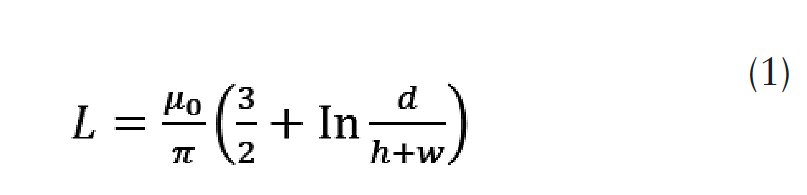
This gives inductance in H per meter loop length. Substituting the values, for a l = 548.64 cm loop length, inductance 4.36 μΗ. the total inductance is, therefore, 14.61 μΗ. 3). The capacitance of a busbar is then ~138.45 pF, obtained by,
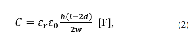
where assuming εr = 60 for an alkaline electrolyte cell (< εr = 80 for water),
III. Methods
A.CISPR 17, S-parameters
CISPR 17 provides a method for estimating suppression characteristics of EMC filtering devices [15]. According to CISPR 17, characteristics of a four ports filter can be evaluated in term of four-port S-parameters using the simulation model as shown in Fig. 4.
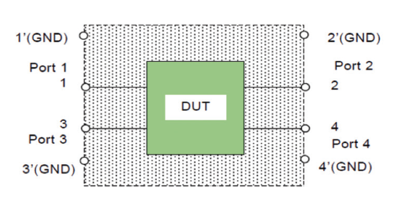
We consider that common mode signals are applied to port 1 and port 3. We drive two expressions for S1 and S3 parameters as the following,
- The wave excitation is ON at port 1 and OFF at other ports (2,3,4), S1 = 1/2(S11+S21+S31+S41) (3)
-
The wave excitation is ON at port 3 and OFF at other ports (1,2,4), S3 = 1/2(S13+S23+S33+S43) (4)
where, S11 and S22 are reflection coefficients, Sij are transmission coefficients (ports: i, j = 1, 2, 3, 4 and i ≠ j)
The common mode transmission coefficient Scc21 is defined as superposition of equations (3) and (4), Scc21 = 1/2(S21+S41+S23+S43) = S21+S41 (5)
The feed inputs and the load end of the busbars are connected to 25 Ω terminations as common mode port references.
B. Maxwell equations for the field
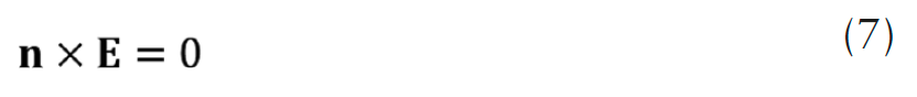
The electromagnetic wave equation for electric field E in frequency domain is expressed by,
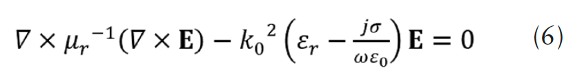
with boundary conditions,
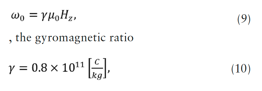
where, εr is relative permittivity [p.u.], σ relative conductivity [1/(Ω.m)], ω angular velocity [rad.s-1], and μr is relative permeability in magnetic core is given in the following expression:
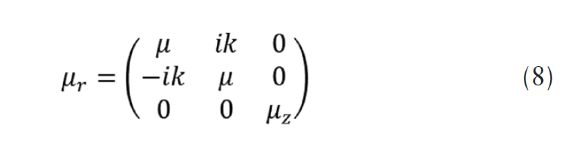
where, index z is chosen to coincide with the direction of the permanent magnetic field Hz
produced by an external source [33]-[35],
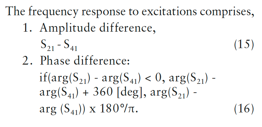
The frequency response to excitations comprises,
IV. Results and Analysis
The S parameters are obtained by solving equation (6) in COMSOL, imposing boundary conditions at the walls of the filter (equations (7)) and parameters (equations (6)-(14)). In the results, the signal being applied is sinus with amplitude (1 V) onto either port 1 or 3. Other ports (2 and 4) are not excited. The parameters S are included into equations (15) and (16) to simulate Amplitude difference and Phase difference. The structure is decomposed into small substructures (Normal mode mesh, Normal mode: (1) Maximum element size: 54.1 mm, 2) Minimum element size: 9.73 mm, (3) Maximum element growth rate: 1.5, (4) Curvature factor: 0.5, (5) Resolution of narrow regions: 0.5.). SMA connectors are used as part of an external interface (Fig. 5).
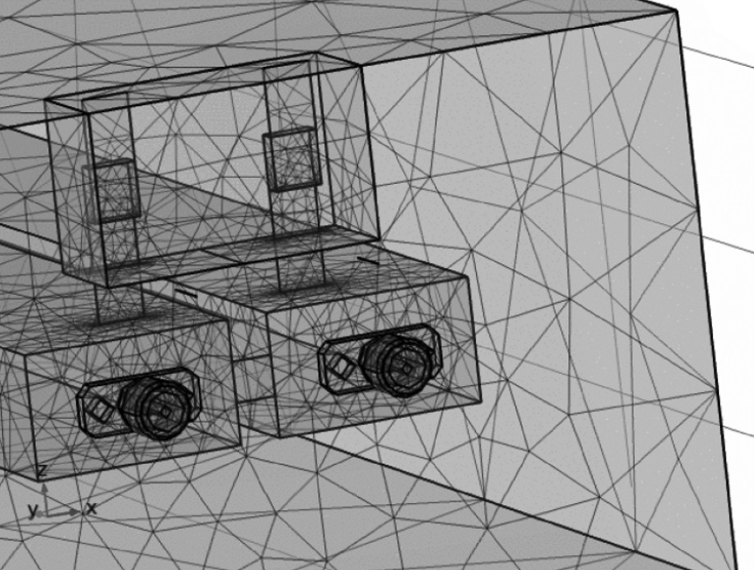
Fig. 6. shows the results for Scc21 as a superposition of S21 and S41 for the busbars when subjected to incident sinus waves (1 V) at port 1. It can be seen from Fig. 6 the lower the input frequency the higher will be the attenuations ( < – 25 dB) along frequency. The shielding B with 86% the area of the original configuration causes its capacitance to vary to a lower value further shifts the pick at 190 MHz towards 220 MHz and affects the quality of signal by -5 dB (< -20 dB, not shown here).
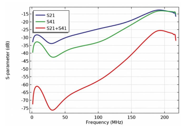
Fig. 7(a) and Fig. 7(b) show the current – frequency and voltage – frequency characteristics respectively as the simulation results for the T-CGC capacitors. The voltage generated over a capacitor is equal to the integral of electric field induced between the plates of a capacitor.
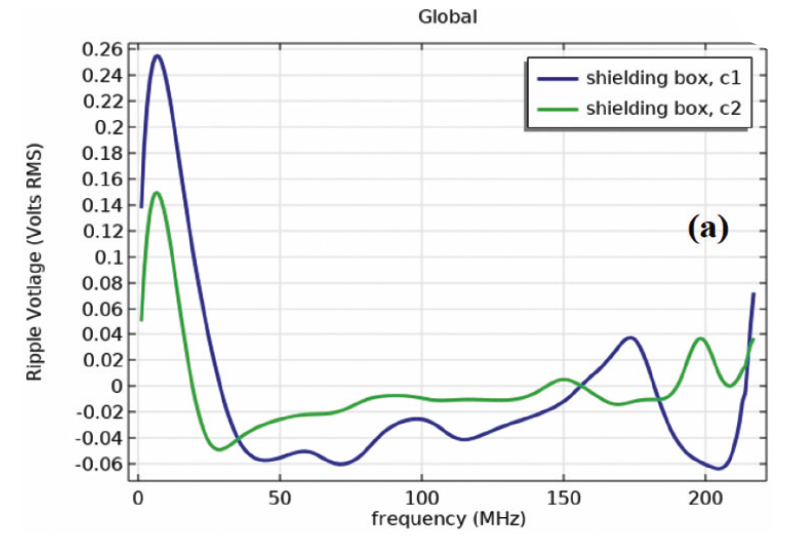
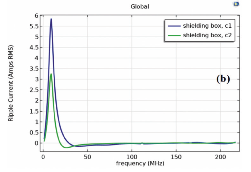
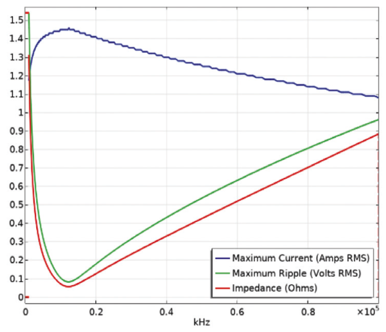
Impedance & ESR VS. Frequency characteristics in Fig. 3 are used to determine the current. As can clearly be seen from Fig. 7(a) and Fig. 7(b), the values of voltage and current are below those corresponding values in Fig. 3.Fig. 8 displays the spatial distribution of the electric field for frequencies (25 MHz, 190MHz, 220 MHz), when subjected to incident signals defined in Fig. 2(c). A large area covers extremely low fields for almost all frequencies as can be easily seen in Fig. 8, in good agreement with Fig. 6. Electric fields tend to cover the whole region at frequency of around 190 MHz.
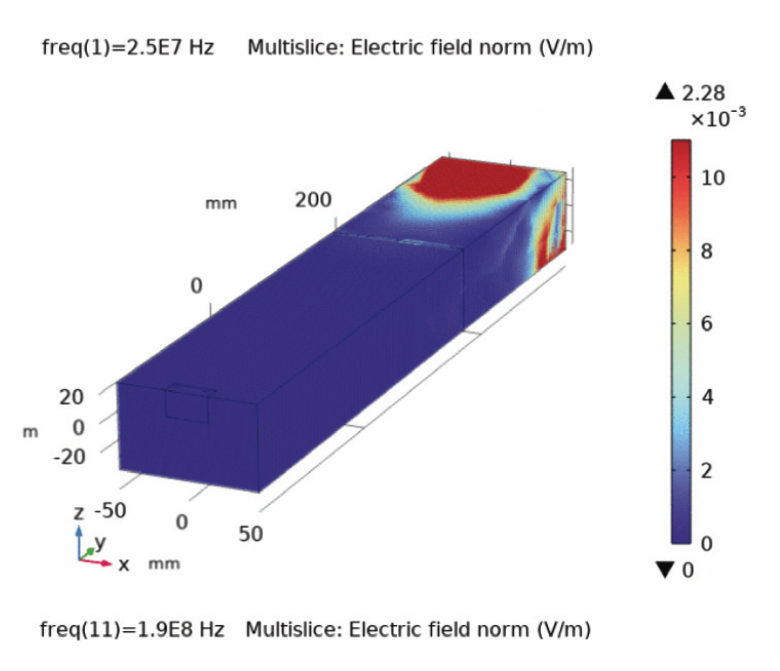
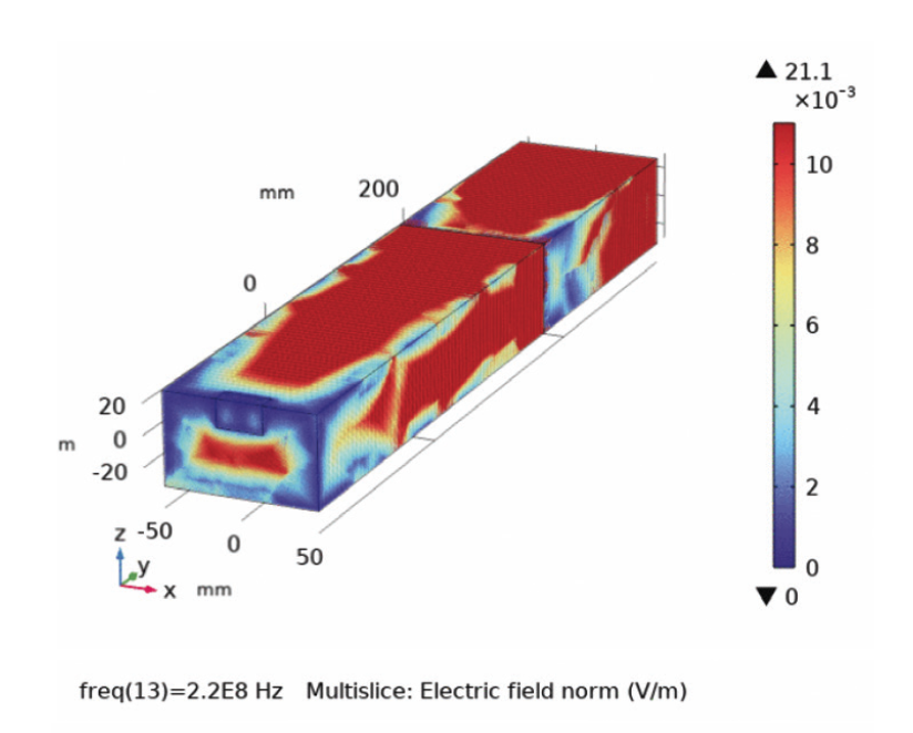
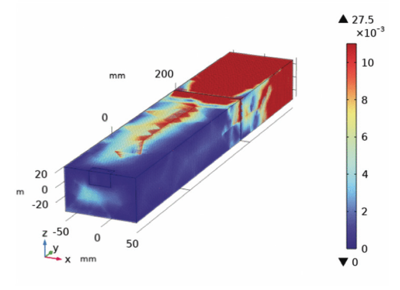
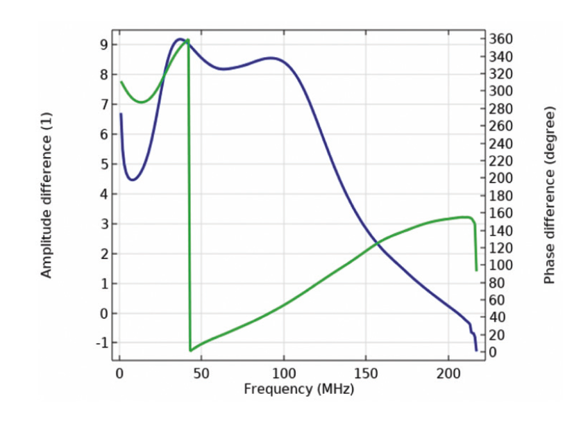
Fig. 9 displays the amplitude and phase imbalancebetween S21 and S41 coefficients. As can be seen, S41 becomes more significant as compared to S21 at frequency 40 MHz. No shift in phase difference appears below frequency 40 MHz and so on until the shift increases linear up to 180 degrees, i.e., sin(Ө) = – sin(1800 + Ө) at 210 MHz. It demonstrates a multi-purpose device operating in parallel as a RLC filter and a fast RF phase and amplitude modulator.
V. Conclusion
A multi-purpose large-scale device (-a RLC filter and a phase and amplitude modulator-) has been proposed comprising two busbars, a UU-shaped magnetic core, and a T-CGC. Faraday shielding is also used to provide protection against interfering signals. The advantages of the proposed design can be summarized as follows,
- The model has been implemented successfully in COMSOL.
- An equivalent parallel RLC circuit model to a battery pack to model and simulate, applied to load, and evaluate the performance of the device.
- CISPR 17 provided a method for estimating the S-parameters for CM.
- Inhanced suppression of CM using grounded shieldings. The shieldings offer con tenuous rejection of CM noise. Significant improvment of attinuations ( < -25 dB) achieved in long frequency range between 1 MHz – 220 MHz.
- Using magnetic iron material with properties remaining extremely stable with relative permeability, frequency, temperature, and applied signal level. Using low capacitance ceramic capacitors use X7R dielectric material that can handle high voltage at high temperature in available space.
- An approach for design optimization of busbars, and spatial positioning of the core.
- The device acts both as a RLC filter and as a phase and amplitude modulator. The core shielding effect is approved to be the reason for phase shifts.
Some improvements are considered by the author,
- Implementing laminated busbars in the design…
- Replacing -63 material with other materials (Ferrites, Amorphous, Nanocrystalline).
- Using COMSOL optimization simulation tools to improve the structure of the device.
- The model can be used for further frequencies and different materials.
- Further works to make: understanding the accompanying differential mode effect and how to eliminate it, a bi-directional large scale RLC filter, following the lumped stray inductance model proposed by [9] where length of busbars and fall times of NMOS transistor revealed in the context.
REFERENCES
- [K. Drobnic, G. Grandi, M. Hammami, R. Mandrioli, M. Ricco, A. Viatkin, and M. Vujacic, “An Output Ripple-Free Fast Charger for Electric Vehicles Based on Grid-Tied Modular Three-Phase Interleaved Converters,” IEEE Trans.on Industry Applications, vol. 55, no. 6, Nov./Dec.2019.
. - X. Hu, W. H. Siew, M. D. Judd, A. J. Reid, andB. Sheng “Modelling of High-Frequency Current Transformer Based Partial Discharge Detection in High-Voltage Cables,” IEEE Trans, on Power Delivery, vol. 34, no. 4, Aug. 2019
. - J. Loncarski, V. G. Monopoli, R. Leuzzi, L. Ristic, and F. Cupertino, ” Analytical and Simulation Fair Comparison of Three Level Si IGBT Based NPC Topologies and Two Level SiC MOSFET Based Topology for High Speed Drives,” Energies 2019, 12, 4571; doi:10.3390/ en12234571
. - J. Meng, W. Ma, Q. Pan, L. Zhang, and Z. Zhao “Multiple Slope Switching Waveform Approximation to Improve Conducted EMI Spectral Analysis of Power Converters,” IEEE Trans. on Eelectromagn. Compat., VOL. 48, NO. 4, Nov. 2006
- S. Park, and T. M. Jahns, “Flexible dv=dt and di=dt Control Method for Insulated Gate Power Switches,” IEEE Trans. on Industry Applications, vol. 39, no. 3, May/Juni. 2003
- G. Giglia, G. Ala, M. C. Di Piazza, G. C. Giaconia, M. Luna, G. Vitale and P. Zanchetta, “Automatic EMI Filter Design for Power Electronic Converters Oriented to High Power Density,”, Electronics 2018, 7, 9; doi:10.3390/ electronics7010009
- E. Rondon-Pinilla, F. Morel, C. Vollaire, and J.-L. Schanen, “ Modeling of a Buck Converter With a SiC JFET to Predict EMC Conucted Emissions,” IEEE Trans. on Power Electronics, vol. 29, no. 5, May 2014
- J. Yao, Y. Li, S. Wang, X. Huang, and X. Lyu, “Modeling and Reduction of Radiated EMI in a GaN IC-Based Active Clamp Flyback Adapter,” IEEE Trans. on Power Electronics, vol. 36, no. 5, May 2021,”
. - M. C. Caponet, F. Profumo, R. W. De Doncker, and A. Tenconi, “Low Stray Inductance Bus Bar Design and Construction for Good EMC Performance in Power Electronic Circuits,” IEEE Trance. on Power Eelectronics, vol. 17, no. 2, March 2002
. - J. Wang, B. Yang, J. Zhao, Y. Deng, X. He, and X. Zhixin, “Development of a compact 750KVA three-phase NPC three-level universal inverter module with specifically designed busbar” 2010 Twenty-Fifth Annual IEEE Applied Power Electronics Conference and Exposition (APEC), 18 March 2010, Palm Springs, CA, USA Charlotte, NC, USA
- H. Yu, Z. Zhao, T. Lu, L. Yuan, and S. Ji, “Laminated Busbar Design and Stray Parameter Analysis of Three-level Converter Based on HVIGBT Series Connection,” 2015 IEEE Applied Power Electronics Conference and Exposition (APEC), 11 May 2015
- F. Zare, and G. F. Ledwich, “Reduced Layer Planar Busbar for Voltage Source Inverters,” IEEE Trans. on Power Eelectronics, vol.. 17, no. 4, July 2002
- C. Chen, X. Pei, Y. Chen, Member, and Y. Kang, “Investigation, Evaluation, and Optimization of Stray Inductance in Laminated Busbar,” IEEE Trans. on Power Electronics, vol. 29, no. 7, July 2014
. - Z. Wang and G. Chen, “Study on Planar Busbar Regarding Stray Inductance Minimization and Oscillation Suppression for High Power Converter,” 2009 IEEE International Conference on Sustainable Power Generation and Supply, 04 December 2009, Nanjing, China
- CISPR 17:2011, international standard, Methods of measurements of the suppression characteristics of passive EMC filtering device
. - Z. Wang, Y. Wu, M. H. Mahmud, Z. Yuan, Y. Zhao, and H. A. Mantooth, “Busbar Design and Optimization for Voltage Overshoot Miti gation of a Silicon Carbide High-Power Three- Phase T-Type Inverter” IEEE Trans. on Power Electronics, vol. 36, no. 1, January 2021
. - H. Wen, and W. Xiao, “Design and optimization of laminated busbar to reduce transient voltage spike,” 2012 IEEE International Symposium on Industrial Electronics, 12 July 2012, Hangzhou, China
- Z. Y. Feng, Z. Zheng, and T. H. Jun,” Study on The Impact of LayerNumber on Stray Inductanceof Busbar,” Applied Mechanics and Materials. Online: 2013-06-13 ISSN: 1662-7482, Vols. 321-324, pp 1439-1442 doi:10.4028/www.scientific.net/AMM.321-324.1439 ˝ 2013 Trans Tech Publications Ltd, Switzerland
- C. Chen, X. Pei, Y. Shi, X. Lin, X. Liu, and Y. Kang, “Modeling and Optimization of High Power Inverter Three-layer Laminated Busbar,” 2012 IEEE Energy Conversion Congress and Exposition (ECCE), 12 Nov. 2012 Raleigh, NC, USA
- A. Hino, and K. Wada, “Resonance Analysis for DC-Side Laminated Bus-Bar of a High Speed Switching Circuit,”, Conference: Future Energy Electronics Conference (IFEEC), 2013 1st International Nov. 2013 21. W. Shen, F. (Fred) Wang, D. Boroyevich, and C. W. Tipton, “ Loss Characterization and Calculation of Nanocrystalline Cores for High-Frequency Magnetics Applications,” IEEE Transe. on Power Electronics, vol. 23, no. 1, January 2008
- N. Igarashi, M. Uozumi, T. Kosuge, A. Sato, K. Kusawake and K. Yamaguchi, “Pure Iron Based Soft Magnetic Composite Core That Enables Downsizing Automotive Reactors,” SEI TECHNICAL REVIEW, no. 80 . April 2015 . 103
- T. E. Salem, D. P. Urciuoli, V. Lubomirsky, and G. K. Ovrebo “Design Considerations for High Power Inductors in DC-DC Converters” APEC 07 – Twenty-Second Annual IEEE Applied Power Electronics Conference and Exposition, 07 May 2007 Anaheim, CA, USA
- Y. Itoh, S. Kimura, J. Imaoka, and M. Yamamoto “Inductor loss analysis of various materials in interleaved boost converters” 2014 IEEE Energy Conversion and Exposition (ECCE), 13 November 2014 Pittsburgh, PA, USA
. - W. H. Martinez,and C. A. Cortes “High power density interleaved DC-DC converter for a high performance electric vehicle” 2013 Workshop on Power Electronics and Power Quality Applications (PEPQA), 30 Sep. 2013 Bogota, Colombia
. - Magnetics – Division of Spang & Company. “Magnetic Cores for Switching Power Supplies”, pp. 1-8. 2009.
. - https://www.micrometals.com/
. - https://www.mag-inc.com/Products/Tape-Wound-Cores/Amorphous
. - A. Abuelm’atti, J. Zafar, I. Khairuddin, A. A. A. P. Gipson, A. Haigh, and I. Morgan “Variable toroidal ferrite phase shifter,” IET Microw. Antennas Propag., vol. 3, Iss. 2, pp. 242-249, 2009.
- B. Lax, K. J. Button, and L. M. Ropth “Ferrite Phase Shifters in Rectangular Wave Guide,” Journal of Applied Physics, vol. 25, no. 11, Nov. 1954.
- B. Foster, I. Gonin, T. Khabiboulline, and A. Makarov “High Power Phase Shifter,” Proceediongs of the 2005 Particle Accelerator Conference, 16-20 May 2005, Knoxville, TN, USA, DOI: 10.1109/PAC.2005.1591385
. - D. Valuch, H. Frischholz, and J. Tuckmantel “First results with a fast phase and amplitude modulator for high power RF application,”Proceedings of EPAC 2004, Lucerne, Switzerland.
. - K. S. Elassy, M. A. Rahman, N. S. Yama, W. A. Shiroma, and A. T. Ohta, “Complex Permittivity of NaOH Solutions Used in Liquid- Metal Circuits,” IEEE Access Oct. 2019; doi:10.1109/ACCESS.2019.2945773
. - C. Kittel “On the Theory of Ferromagnetic Resonans Absorption,” Physical Review, vol. 73, no. 2, Jan. 15 1948.
. - T. L. Gilbert, “A phenomenological Theory of Damping in Ferromagetic Materials ,” IEEE Trans. On Magnetics, vol. 40, no. 6, Nov. 2004.
- P. S. Epstein, “Theory of Wave Propagation in a Gyromagnetic Medium,” Reviews of Modern Physics, vol. 28, no. 1, Jan. 1959.