


In production . of printed circuit boards (PCB) signal skew will be introduced in differential traces due to the weave effect. A skew that will vary from PCB to PCB. This signal skew generates mode conversion that together with poor common mode properties, along the high-speed channel, will degrade the system performance. For example, might the skew effect give a crosstalk much higher than the pure differential crosstalk. If the poor common mode properties in the channel are high and the skew can be expected to be high enough, the channel performance will be affected. Some PCB’s, with right combination of skew, might fail with too high bit error rate (BER) and other PCB’s will work.
I . Introduction
In high speed serial links are often components as connectors and via structures included. Such components and structures might have poor common mode properties. The poor common mode properties will not influence the differential signal as long as there is no common mode signal generated along the channel but influence if common mode signals are introduced. Signal skew is a large source of mode conversion to generate common mode signals in the channel. This common mode signal might have a large impact on the performance due to the poor common mode properties in the channel. This paper will discuss mode conversion, coupling mechanism and its impact on the performance.
II. Skew and mode conversion
Mode conversion can be generated by several sources. Sources as signal skew, impedance mismatch, geometric differences in traces and stackup, non-symmetrical driven signals out from a transmitter, mismatch in transmitter and/or receiver termination impedance, imbalance in placement of ground vias around a differential pair via, imbalance in the signal path through a connector etc. But normal will the skew generate the highest mode conversion. All other mode conversion is normally small compare to skew in high speed links.
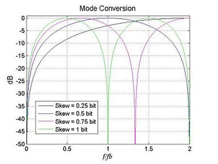
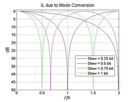
Fig. 1 shows mode conversion caused by skew in the coupled transmission line. The transmission line is a stripline with equal propagation velocity for differential mode and common mode signals. On the x-axes is f/fb scaled where f is the frequency and fb is the baud rate. On the y-axes is the amplitude in dB. With a skew of one bit will all off the differential signal be converted into common mode at half baud rate. Fig. 2 shows the differential insertion loss (IL) after the skew. With a skew of 25% of the bit length, approximately 10 ps in a 25G link, gives 0.7 dB in IL at half baud rate. But with a skew equal to one bit will create very large IL, in theory infinitely large, at half baud rate. With a skew of one bit and a transmitted data patter of 1.0.1.0.1.0… will not pass the link as a differential signal, it will show up as a DC-signal, a common mode signal, at the receiver. This does not mean that a channel with a skew equal to one bit or more will not function. The decision feedback equalizer (DFE) [1], in the receiver can, to a certain extent, reshape the signal to a useful signal pattern.
For example, in a link with a one bit skew and the n-channel lag the p-channel. If now the DFE cancel out the contribution from the n-channel at each sampling point. Then will the receiver only see the p-channel with, for this example, is the bit pattern 1.0.1.0.1.0… This handling of the skew, in DFE, works only for the part of the lag pulse that is within the DFE working range. The signal will however suffer from extra losses, the signal will be approximately half in amplitude with one bit skew, approximately 6 dB extra loss, compare to a channel without skew.
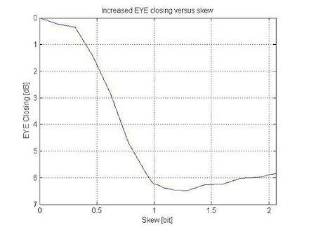
Fig. 3 shows the increase in EYE closing after DFE verses skew length. The link, in this case, has an IL of 20 dB at half baud rate and the graph shows the extra introduced losses, caused by the skew, after the DFE. With a skew of approximately one bit or more the increase in losses is about 6 dB. This type of losses will, in many cases, have rather low influence on the noise in the channel if we exclude crosstalk noise. But with margin for the extra losses and the increase in noise, caused by the skew, a channel with skew of one bit or more will work.
Mode conversion converts, for example, parts of the differential signal into common mode signal. If this common mode signal reaches the receiver the receiver can normally handle this common mode signal without too high disturbance. The mode conversion in the receiver is normally rather low.
III. Skew combined with crosstalk
In the section II it was shown that common mode effects caused by skew will, in many cases, be of no problem, the DFE take care of the skew effects. Often will the common mode effects be ignored or add little attention to in the design process. With low attention on common mode properties often large or very large common mode crosstalk and common mode impedance mismatch can be observed in channels. It’s rather common to see plus 20 dB of higher common mode crosstalk compare to differential mode crosstalk in connectors, via structures etc. So, for example if there are a skew, on an aggressor line, in front of a connector, and the connector suffer from high common mode crosstalk then will the victim channel get a high common mode crosstalk signal. As the receiver is rather insensitive to common mode signal this common mode crosstalk signal will normally be of no problem.
If we now have two sections with mode conversion in the link one on the aggressor channel in front of the connector and one on the victim channel after the connector, see Fig. 4.
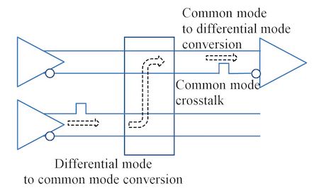
In this case will the signal convert to common mode in the aggressor skew part and feed the connector with common mode signal. This common mode signal will leak into the victim channel and at the skew part in the victim channel, after the connector, will this common mode signal convert back to differential mode and show up as a differential crosstalk at the receiver. A differential crosstalk, coupled as common mode crosstalk, added to the pure differential crosstalk. If for example the common mode crosstalk is 20 dB higher than the differential mode crosstalk and a skew of 10 ps exist at both sides of the connector in a 25G link (about -8 dB in mode conversion at half baud rate, see Fig 1) then will the differential crosstalk, caused by the skew, be -8 dB + 20 dB -8 dB = +4 dB. This crosstalk caused by the skew will be 4 dB higher than the pure differential crosstalk and then dominate the crosstalk picture. The skew effects can not be neglected if the common mode crosstalk is high compare to the differential crosstalk.
In a crosstalk section is normally also a mode conversion taking place, a conversion from differential mode to common mode. For some skew settings on the aggressor channel will this mode conversion and common mode crosstalk be in phase and add up. For other skew settings they will cancel out each other and reduce the output common mode signal. The skew on the receiver channel will also be in phase or out of phase of the common mode crosstalk signal. This crosstalk, caused by the skew, is added to the pure differential coupled crosstalk. The phases of the crosstalk caused by the skew and the pure differential coupled crosstalk will strongly influence the total
differential crosstalk. To find the worst crosstalk situation different combinations of the aggressor skew and the receiver skew must be investigated. One skew combination will give highest crosstalk in one frequency area and another combination might give highest crosstalk in another frequency area.
The mode conversion from skew takes place at the edge of the signal transition. If there are two skew sections together with a common mode crosstalk coupling in between and the skew is short compare to the pulse width. Then will the differential crosstalk signal, out from this skew section, be a sinusoidal pulse shaped signal generated on each signal transition. The period time of the pulse will be close to the bit length. The spectra content of this pulse train will be high in frequency. The majority of the crosstalk noise power will be around 10 GHz in a 25G link. The level of common mode crosstalk around 10 GHz is then very important for the crosstalk coupling caused by skew.
IV. Structures with high common mode crosstalk
The common mode crosstalk takes place in different types of structures. Listed below are some structures that suffer from high common mode crosstalk.
Microstrip routing; Tight routed differential microstrip traces will have a rather high common mode crosstalk much higher than stripline. Microstrip routing needs then larger spacing to minimize common mode crosstalk. Microstrip has also different propagation velocity for differential mode and common mode signals. A length compensation is then needed to be placed close to where the length mismatch occurs otherwise will the differences in speed make the length compensation not to work.
crosstalk
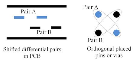
Spatial shifted differential pairs to minimize differential crosstalk; Sometimes one sees recommendation to spatial shift traces to minimize differential crosstalk or to place vias and pins in an orthogonal configuration. Fig. 5 shows two examples of this type of arrangement. Both have low differential crosstalk but high common mode crosstalk. If for example the shifted differential pairs are used in a PCB layout and the length of the coupled section is 10 mm. The differential mode crosstalk will be low but the common mode crosstalk will be very high. Fig. 6 shows the differential near end crosstalk, NEXT, with 40 mm traces between the aggressor and the coupling section and 40 mm traces between the coupling section and the receiver. The skew, of 10 ps or 20 ps, are placed equally on both the aggressor side and on the receiver side.
The differential crosstalk, at close to half baud rate, increase with almost 24 dB with 10 ps of skew and almost 30 dB with 20 ps of skew compare to the situation with no skew. For such layout, for high speed links, will reduce the operational margin for a system when skew is introduced. Some connectors use this shift arrangement of pins inside the connector to minimize the differential crosstalk. The connector will then suffer from very high common mode crosstalk.
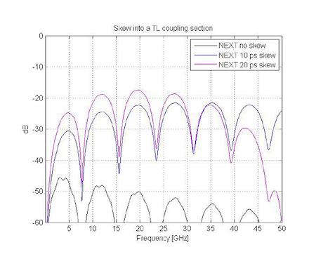
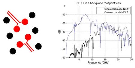
Fig. 7 shows a rather common used via pattern for connectors. Here is the signal vias as red and ground vias as black. To the right is the differential mode NEXT and common mode NEXT plotted. The common mode NEXT is about 30 dB higher than differential NEXT in a large frequency range. The thickness of the backplane is 4 mm.
Ground return path inside connectors; To maintain a good current return path for common mode is difficult inside a connector. There should be a ground that encapsulates all the electromagnetic fields from the signal pins. There should be no leakage of fields between differential pins and to get this a 360° shield should be placed around each differential pair. But in the mating area is it difficult to maintain this field encapsulated structure. Often the ground structure starts to get a shape of a pin or the structures got holes and cut outs. Also at the side of the connector is it difficult to maintain the 360° shield. Through the openings in the shield will the fields leak and create crosstalk. Especially the common mode fields will leak through openings as all common mode fields will be terminated to the ground shield.
V. Sources of skew
Skew can be created in different ways in a link. Listed below are some structures that can generate skew in a channel.
Different trace length within the pair; Mismatch in length will create skew. Stripline will generate approximately 7 ps skew per mm in length difference. Layout tools have support to avoid mismatch in length so this is normally in control. But it is important to compensate length differences prior entering vias etc. because differential mode and common mode have different velocity through a coupled via and a length compensation after a via will then not work. One need also be careful in length compensation for microstrip. Microstrip has different propagation velocity for differential mode and common mode signals. To eliminate introduced length mismatch the compensation should be placed close to the where the length mismatch is generated otherwise will the differences in speed make the length compensation not to work.
Weave effects; The dielectric material used in PCB consist of resin/epoxy and glass fiber weave. The electrical properties of resin and glass weave are different and give an inhomogeneous dielectric environment. Normal used glass has a dielectric constant of 6 and the resin has a dielectric constant around 3. The glass weave consists of woven fills and warps. These fills and warps are as bundles if they are not spread out. A trace placed over a bundle will se higher dielectric constant than a trace placed between two bundles, see Fig. 8. The lower trace will see a higher dielectric constant than the upper trace. The differences in dielectric constant generate a skew due to the difference in propagation velocity for the traces.
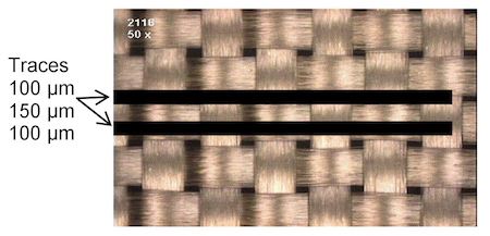
A dense weave as 2116, 7628 etc. gives smaller variations in the electrical environment. A more open weave gives larger variations. Reference [1] and [3] gives indications that a skew up to 9 ps/25 mm might be expected for dense weave. With longer traces parallel with the weave higher skew will be expected. The level of skew will vary from PCB to PCB and must be treated as a probability function. If for example the total lengths of traces that are parallel with the weave are 30 mm or longer then can we expect, to a certain probability, that the skew will exceed 10 ps and for traces longer than 60 mm the skew will exceed 20 ps.
One way to minimize the weave effect is to route the traces with an angle to the weave, to avoid 0°, 45° and 90° angle to the weave. But this type of routing need larger area on the PCB and this area might not exist. Also in the breakout area of integrated circuits and connectors it might not be possible to place traces in a non 0° and 90° angle fashion. To rotate the PCB on the panel might reduce the utilization of the panel and increase the PCB cost.
VI. Conclusions
Skew is a major source to mode conversion, a conversion from differential mode to common mode signal and vise versa. Often are component/structures in a channel with poor common mode properties used. For example, a component with very high common mode crosstalk. If there is a new mode conversion after the common mode crosstalk then will this common mode crosstalk signal be converted into a differential signal. This differential crosstalk signal, passing as a common mode signal through the component, can be much higher than the pure differential crosstalk.
The skew will vary from PCB to PCB and the crosstalk level will then vary from PCB to PCB. If the link passes a backplane or a cable the combinations of PCB’s will set the crosstalk level. One combination of PCB’s might fail due to high bit error rate caused by the skew combinations. By exchange one PCB the link will probably work again. This, from PCB to PCB, random crosstalk level is hard to investigate and difficult to find the fault if one board is pointed out as faulty.
Common mode properties in connectors, via structures etc. together with assumptions of skew levels should be considering in the analyze of a link. To ignore the common mode effects might give high fault rate in volume production. The supports from simulation tools to handle skew in links are normally limited and require large man work to cover.
Ingvar Karlsson Ericsson AB
References
[1] Dianyong Chen. SerDes Transceivers for High-speed Serial Communications.[2] Eben Kunz et al. Oracle Corp. Sources and Compensation of Skew in Single-Ended and Differential Interconnects. DesignCon 2014.[3] Peerouz Amleshi et al. Molex Inc. Intra-pair “Unaccounted” Skew Effects and Suppression. DesignCon 2014