

Detail EMC design . This article is a part of a series of texts that will deal with the EMC challenge in terms of project management and the practical EMC activities at different stages in the project flow.
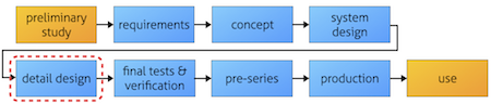
Different companies all have their own way of describing their project flow, so to keep it simple we will use the labels as given in Figure 1. We can call it a generic project flow. The picture only describes the basic outline of the work packages. These articles will describe the actual practical work we want to do in the project to “make EMC work” in a time- and cost-efficient way. Each part of our series will fill in the details for each part piece by piece.
This is the 5th part – Detail EMC design – in our process picture.
We have previously looked at the EM environment, requirements, possible disturbance risks – resulting in an overall plan for the EMC system design. It is now time to distribute the work to the design groups for the different system components and see the practical outcome of all the preparations. We are finally building something – on solid EMC Analysis Ground.
The content of detail EMC design
There are many articles and books on how to do detail EMC designs on various product levels. So, instead of discussing what capacitors to use and how to place them on the PCB (indeed very interesting, but I will restrain myself) I will describe my view of the structure of the work and how it can be arranged to allow the designers to have a good night’s sleep.
The basic approach
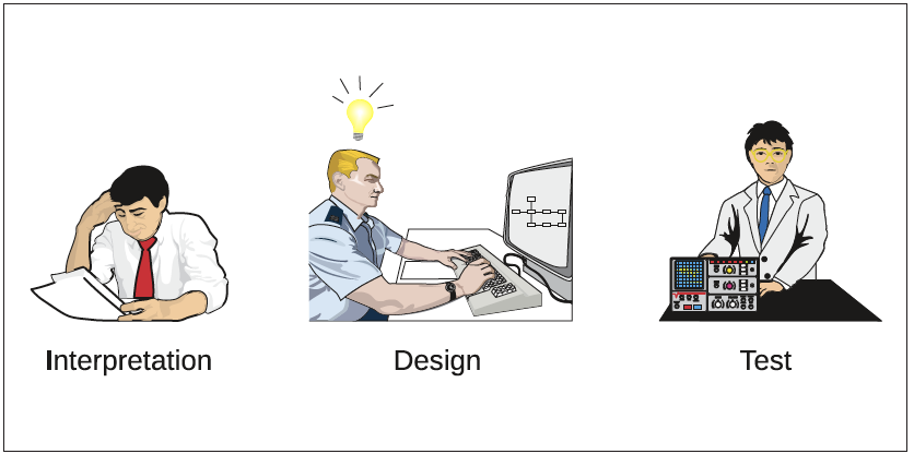
The work can be summarized as in Figure 2. The designer’s objective is to fulfill the requirement specification at the verification test. That phrase contains two important parts:
- The requirement specification. If I do not know the requirements, how do I know what to design? So, it must be stated in a form that is usable for the designer
- The test. If we are about to do some testing, there must be a description of how to do it – the EMC verification plan. That part was covered in the previous article (system EMC design), so I now have access to that document.
To make the work efficient, we will now make use of all the preparations we have made in the previous project phases. In addition, we will now also get results from our early design tests which will show us if we are on the right track.
Follow the flow
When I have been participating in design projects, I have found it most useful to interview the designers and put a very simple question: how does it work? That may sound like a very naïve question, but that question allows us to step back and look at the big picture. How does the information flow through the component? By looking at the information flow, we can place the sub-components (processors, memory circuits, interface circuits etc.) where they create the minimal routing on the PCB. We can also try to rotate the circuits so that the pinout matches the information flow in a better way. The same can be done on the next level if we have multiple PCBs or other components. The result will be better cable routing and shorter harnesses. In addition, we can differentiate between internal cables and those who will face external connectors (to other system parts). All together, we get a more robust design at the same time as we reduce internal crosstalk and the size of the unintentional antennas.
On top of this we have all the design details that will be governed by the corporate design rules and our experience from previous projects.
Using the EMC verification plan for design
If the verification plan is relevant for the real-world risks, then designing to meet the requirements is relevant. If it is not, we might fool ourselves into believing that we make a robust design – but are stepping into the trap of surprises during the final EMC verification.
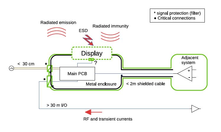
But let us assume that we have written an EMC verification plan of high quality. We bring it forward and study how the tests are to be performed. A simplified view is shown in Figure 3.
The component has 3 signal cable interfaces with different requirements. The longer cable will be exposed to high energy transients, so it will need a robust transient protection. The short cable will not be tested with any specific cable tests, so the remaining threats to take care of are RF emission and immunity (radiated). By stating (as given in the previous system design) that the interfacing component is isolated, we avoid the risk of having galvanic injection of transients etc. The third cable is shielded and short, which means that having a proper shielded connector will handle the RF challenge. If there is no test or requirement specified on the inside of the shield – there will be no protection provided. But maybe there is a need for specification of the ripple on inside of the shield? Flaws in the verification plan may be discovered, and by reporting them the specification will be updated. The mistake will be added to the lessons learned, and the next project will be even better.
In addition to the radiated tests, we also find an enhanced requirement on ESD immunity. This will be important when looking at the display design. The item is transferred to the purchase review, described further below.
Finding the details of EMI risks
Using the EMI risk analysis is an activity that is integrated in the total design work, including the incorporation of the verification plan information. I have listed it under a separate heading just to emphasize a few items. The aspects are included in Figure 3.
In the making of the EMI risk analysis, an efficient method is to create a Common Mode (CM) schematics – seeing the invisible unintentional currents. When we get into the physical detail design, it will be easier to identify what parts we are talking about and where these currents may flow. We do not want these currents to rush through our sensitive circuits, but rather guide them into a safe route – e.g. via filtering to the reference ground (the shield for the system). That way, critical connections are identified from the risk analysis, and this is good advice that will influence the technical details on filter assembly etc.
Now, the display is sort of hanging loose in the zone boundary – or is it? That depends on its design, which we have not yet seen in detail. Shall there be a filter on the PCB-to-display cable? That is an item to evaluate during pre-compliance test! I will add this aspect to the EMC design check list and discuss it with the EMC review engineer.
Design reviews
As I previously described in article 3 (The concept phase), an EMC design review can be regarded as an EMC test, where you are replacing the laboratory with an experienced EMC engineer. At this stage, you dig more into details in your design reviews – what to change and based on what arguments. A great advantage with these reviews is that you can start with them very early. They are not dependent on functional subsystems or software!
In the reviews, you are checking the borders, using the zoning analysis. Use the map that you have! Do not hesitate to make improvements of the map. Just be sure to communicate the changes to those who are concerned.
In this work, we check critical connections and component choices, avoiding shunting of blocking devices etc. the analysis is made on both mechanical installation of e.g. PCBs and cables, partitioning and component placement on PCBs, routing, and enclosures (also the plastic ones). The resulting comments and assessments can be summed up in a design check matrix for better overview, and also to make follow-ups easier and faster.
Checking purchased items
Some parts are not designed in-house but bought as a readymade sub-component. When doing so, it is very important to check its EMC properties. That review should not be limited to checking if it meets the same EMC standard as the one assigned to the complete product. We want to know if it will fit into our EMC design strategy. In our case, we will buy a finished display. So, we begin with looking at the EMC specification for it – with a particular interest in its susceptibility for ESD, since it was highlighted in the EMI risk analysis.
In the case of using a shielded cabinet as a design solution – as the shielded cable suggests – we also want to check how the display can be assembled as a part of the shielded design. It is also good to ask the supplier for detailed information on how testing of the display has been made (which should have been made since there are EMC properties described). If you get some answers, you can check if the supplier´s testing meets your design assumptions. If you do not get anyanswers, that is a warning signal urging you to make a design test with the display included very soon. Depending on what you get, you can
- Review test results that have been obtained and assess how large margins you may have
- Assess the test methods used – if they differ from what you wanted
- Check that the testing is made under conditions comparable to your own product. E.g, they did not make the test with a shielded power cable (that was the case in a project I took part in, and it surprised my client quite a lot).
- Ask for modifications on the item you want to buy
- Find another supplier
Pre-compliance testing
Using the results
In the design tests we get the first compliance status on the selected preliminary tests. With this feedback to the project we know where we are heading and can make corrective actions (well, we will most certainly find things to change). The results will also be valuable information to the design reviews, so these two activities shall be planned closely together. It is important not to forget the good ideas on design solutions that will come up, so the design reviews are good opportunities for documenting and keeping track of progress – e.g. by updating a design check matrix or equivalent.
The content of the pre-compliance testing is prepared long time ago – in the concept design phase where we made the first EMI risk analysis. In addition, when using the risk analysis in the detail design work we have already prepared for a set of experiments to find the best way to handle the risks. The value of the pre-compliance testing will then be even higher. Which design modifications worked? Did not work? Are some designs overkill? Shall we keep some of the modifications as safeguards for the final testing? It is always good to have some aces up your sleeve. By knowing them in advance, they could even be prepared for production (such as zero-ohm connections at your connectors that can be replaced by ferrites).
In these first tests, be sure to also include some type of immunity test and not only emission measurements. You may find that the product behaves in a way that was not at all expected (such as latch up or overheating), and some of that may be related to your software. The result is that you learn more about the robustness of the product, and it may also result in that you will have to update your pass/fail criteria.
Improving your test configuration
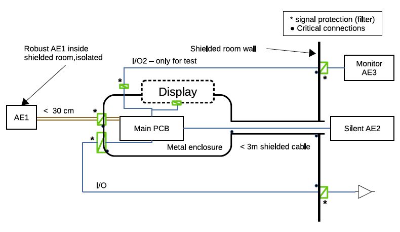
We use the existing verification plan and put it to test. Will it work? We will most certainly learn more things about the product, and consequently more about how to test it. So, it is a good exercise for the future final verification test. We update our figure of our design from Figure 3, and add the test adaptations into Figure 4. The figure shows a presumed test setup in the shielded room. Other setups will also be prepared for, but let us take this one since it is often the most common one design engineers discuss. We now find a set of aspects to handle:
- An additional signal interface (I/O2) is needed for the monitoring of the performance of the Equipment Under Test (EUT), and it needs protection
- The short cable shall have termination corresponding to a component we do not have access to. We will replace it with an Auxiliary Equipment (AE1) that will be placed within the room and must therefore be of higher quality than the EUT
- We need an AE2 to simulate the adjacent system inside the shielded part of the system. We do not want a failure due to that system, so it needs to have a silent design. It is put on the outside of the shielded room, and it could have a high-grade filter. Space and cost are no issue here – we will only build one.
- The shielded cable must be longer than in the actual installation to fit the room, so it must be specially tailored and built
- We need to make sure that the intended EMC laboratory has the interfaces in the shielded room that works for us.
Adapting the EUT for test
When we perform the EMC testing on the EUT we want more detailed information on the behavior of the EUT than in normal use. We also want to have efficient use of testing time, so the execution of operating modes (often several ones nowadays) need to be speeded up without introducing irrelevant behavior. This calls for a dedicated test software (SW), and guidance in making this SW shall have been generated in the system design phase.
We will often need additional hardware (HW) interfaces for the monitoring of the behavior (the I/O2 in Figure 4). This must be fitted into the EUT from the beginning, but the necessary filtering and protection does not necessarily have to be within the EUT. If designed properly, a short unfiltered cable can be used as long as it will not be an unintentional antenna within the frequency range measured.
Input and output
As a summary, we find the following interface conditions to the other parts of the project flow.
Input from previous work:
- System concept design
- Zone description
- EMC verification plan
- EMC design check matrix
- Best practice EMC design – design rules
Output from this stage:
- Prototypes for testing
- EMC pre-compliance test reports
- Updated EMC design check matrix
- – From the EMC design reviews, now with more details
- – including reviews on critical purchased components
- Compliance matrix
- – Updated with status from pre-tests
Closing remark
During this project phase, the EMC issue is becoming more real to us. In particular, the pre-compliance testing is very good to use to get attention to possible future verification failure – in particular if you want project management to listen.
But work is now often hectic, and you tend to focus on critical issues that you are facing right now and EMC may not be one of them. My point here is that you do not get more time to solve the EMI issues later on in the lab – rather the opposite. In addition, troubleshooting cost in lab is about twice as much as design work in the office. To find an efficient way forward you need to allocate time to specific EMC activities such as described above. By using the prepared information and tools that have been created in the previous phases, now is the time when you are avoiding mistakes and are saving time and money for real.
Lennart Hasselgren, Lic Eng.
EMC Services, lennart@emcservices.se If you have ideas and comments on this article, please feel free to mail me! Some might also recognize my short examples, and if you want to add something that would be an interesting talk.