

Preamble: . As for any organized EMI control, ESD protection consist in anticipating or correcting the unwanted effects of an hostile electromagnetic ambient. Like many EMI threats, ESD manifests through conducted and radiated phenomena, with the latest being often the dominant mode. But there is a unique aspect to ESD, not found in common radiated EMI episodes where the victim box and cables are illuminated by a uniform field. Instead, ESD generates locally a strong field pulse, typically > 1kV/m near the discharge point, dropping quickly as one move away. Therefore, although ESD hardening should be part of a general EMI control, not handled as a separate constraint, some classical EMC solutions may not be sufficient and should be complemented by additional protections.
Looking at Fig . 1, ESD immunity can be considered at the following stages:
- At component level
- At circuit board level
- By software and noise cancellation features
- At internal packaging & wiring level
- At housing/cabinet level
- At installation and environment level
In theory, one could implement a full ESD protection at one of those levels only. Yet, costwise, it is more efficient for ESD control to be shared between several levels. Like the skins of an onion, there are several layers, from the physical envelope (metallic or not) of the product down to its active center core (the ICs that perform the essential functions). Each layer corresponds to a certain power level and frequency band of the signals being handled. For instance:
– Going from the external envelope where inputs/outputs can handle tens, or eventually hundreds of Volt, like for power supply, levels as low as 1Volt and few tens of mA are reached after a few layers, when getting to the chip core.
– In terms of frequency, the functional bandwidths range from kHz for low speed analog up to hundreds of MHz, eventually GHz with high speed digital processing.
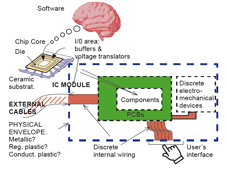
Whatever based on clamping, filtering or shielding, no single device, regardless it protects from damage or prevents errors/signal alterations, can perform alone for all these different amplitudes and frequency domains. Instead, protection elements are best installed at the boundary of these layers, with current handling capacity, bandwidth and physical size that are commensurate to the layer which is to be protected downstream.
1 . ESD protection at component level
A first degree of ESD immunity can be achieved by selecting components (logic or analog ICs, operational amplifiers, resistor networks etc..) that already have built-in ESD protections.
1.1. Integrated Circuits with internal ESD protections
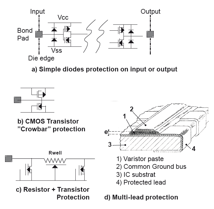
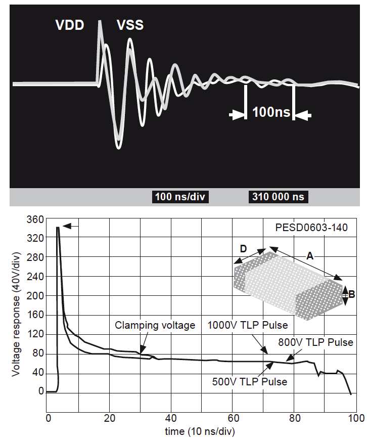
Thanks to the huge growth of the ICs market and the need for cost/size reduction, manufacturers are now integrating some ESD protections in the chip itself. However, as often, this is conflicting with an other trend: Size reduction, by shrinking the IC features down to the sub-micron region, results in thinner oxide thickness and traces width, such as even the protection devices like diodes, crowbar transistors and polysilicon resistors can no longer handle the ESD pulse energy. The efficiency of these techniques are evaluated through the standard ESD tests, or a more recent evaluation tool: The Transmission Line Pulse (TLP), injecting a calibrated square pulse into the device via a RF-type jig. By varying the pulse amplitude / duration, more insight is obtained for critical failure parameters of each IC pin, including I,V curves and mismatch. This is simulated by software tools, with results correlatable to those of a real test pulse.
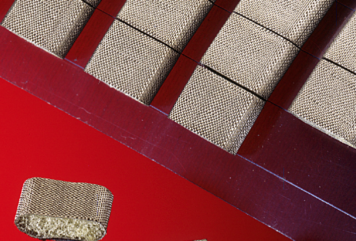
An other need urged IC manufacturers into designing overvoltage suppression: the Latch-Up, typical of CMOS, but also found with bipolar technologies. It manifests as low resistance path, bridging Vdd with Vss if a transient current exceeding few 100mA is applied, generally ending-up in IC damage by overheating. Some passive overvoltage protections can be built-in the chip. Others have been devised, which are not integrated in the chip but implemented in the module package, hence do not suffer the same dimensional restrictions, like ZnO varistor ring laid on the periphery of the chip carrier or substrate Fig. 2. Efficient integrated protections, up to 15kV, are achievable, but at the expense of chip real-estate. High speed I/Os can be protected on the chip, but at some prejudice to their speed, due to the capacitance of the integrated diodes. If no technology or vendor can be found with built-in ESD protection that matches the objectives and constraints, application-specific protections are necessary. This is especially true for lines which are connected to “user-touchable” items, mostly connectors, as explained next.
1.2. Additional ESD protection; When is it needed, and how much?
Rather than adding external Transient Voltage Suppressors (TVS) to each component, purchasing parts which are ESD-immune (for instance with a 2kV to 4kV ESD grade) is cost-effective. Yet, in many cases, an additional protection is necessary, selected to fulfill the expected ESD immunity of the equipment, because:
a) Integrated resistors, zeners and crowbars are efficient against damages but cannot prevent errors due to few volts transients induced by ESD.
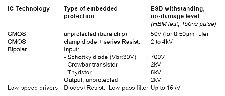
b) The 2kV or 4kV vendor-specified immunity is only granted against a human body (HBM) discharge, with a maximum current of 2.6 A (for a 4kV grade). This covers the IC during handling, manufacturing assembly, packing/unpacking or maintenance. In actual machine life, and during ESD tests, ESD currents up to 30A, for 8kV(direct contact), and 45A (air discharge) can be stressing the equipment. Most circuits will never be directly exposed to such currents, but some will, like ICs that connect directly to a user-touchable connector pin, manual switches, etc … or that are arc-reachable (air discharge).
These added protections can perform by:
– decoupling (clamp diodes, crowbars and capacitors): the current is bypassed to Gnd or +Vcc
– blocking (inductances): A high impedance is opposed to the ESD current
– absorbing (lossy ferrites and resistors): The ESD pulse is dissipated into heat.
Depending on the selected components, their action can:
– insure a damage-free, but not an error-free operation, or
– filter the high frequency part of ESD spectrum, hence preventing errors with short pulses (<10ns), but cannot attenuate long ESD pulses, typical of a direct injection, or
– insure both survival and error-free protections.
Following are commonly used ESD protection components, mounted close to the IC to be protected:
a) TVS (discrete or integrated). Leadless SMT devices, with 2 to 8 terminals are available (Fig.3), handling the full current of a 15kV IEC-type discharge.
b) Series resistances limiting the current on the sensitive, high impedance inputs.
c) Capacitive decoupling next to critical signal pins. On signal inputs, 30 pF or more can be added, depending on what capacitive loading is tolerated by this line w/o affecting the performance. While transient protectors do not eliminate low level glitches (those not high enough to cause damage, but exceeding the detection threshold), decoupling capacitors will.
d) Capacitive filtering next to the power input pin. A 100nF ceramic capacitor can be added, even if not considered necessary at the initial circuit design (some Vcc supply pins can cause a logic error if the parasitic pulse has enough amplitude). There is now a general trend among IC manufacturers to incorporate such capacitors in the chip itself, using diffused junction capacitances.
When cascading external clamping devices with chip internal protection diodes, watch for clamping coordination: If a fast acting diode exists already inside the chip, it parallels the external clamp and one must make sure that the first one will not react faster. This would cause the faster but fragile device to prevent the triggering of the bigger one, and to be destroyed by an energy that it cannot handle. Always place some series resistance or a small inductance between the two.
A last advice is to make sure not to use a too fast technology, unless it is absolutely needed for a specific function. Often, logic families with 2 or 3ns transitions are used all over the board, assuming that ”the faster the better”.
2. ESD protection at the PCB level (Internal Circuitry)
The printed circuit board is the area where the improvement/cost ratio is the largest. The effort invested in sound PCB layout will be paidoff times over by a gain in immunity which can be drastic, often at no additional parts cost. There are many cases where ESD immunity was built at PCB and I/O levels so that even without additional shielding of the housing, the equipment withstand ESD levels above 10kV. The guidelines given here are a short compilation of time-proven, non self conflicting rules, that build-up the ESD defense at no prejudice to EMC or product performances, because they all concur to high immunity and low emissions, up to > 300 MHz.
2.1 Reducing the field-to-PCB coupling mechanisms
Beside the direct contact by the ESD intruder, two ESD field-coupling mechanisms are playing a role in the PCB susceptibility, as described before: H-field coupling and near E-field (or capacitive) coupling.
a) Against H- field coupling: the rule here is to minimize the exposed loop areas by checking all the runs against signal-to-return loops or Vcc-to-zero-volt loops (Fig. 4):
- No signal or Vcc trace should run without a close Gnd return (trace or, preferably, plane): Use ground planes or largest possible copper lands, to act as noiseless ground and shield. Double-sided boards with maximum un-etched copper on one side are better than single-sided boards, multilayers being even better.
b) Against E- field coupling: Here the risk is some invisible capacitor between the PCB and the charged source: the gun tip, the edge of the HCP or VCP during the test, or a person’s finger during an actual event. Any exposed sensitive trace, high impedance IC input, or IC package itself can capture a capacitive current during the abrupt ESD voltage change. Such target should be protected by a ground plane underneath (or above):
- Minimize the length of open-ended high impedance lines.
- Do not allow unused inputs to be floating, hence making easy targets for capacitive pick-up.
- Never run critical signals (Clock, Reset, Watchdog etc … ) near the board edge. Such locations are prone to capacitive coupling from a nearby ESD. This applies even to PCB with full ground planes, since copper planes themselves are often etched near the edge of the epoxy board.
- For reinforcing the screening effect of the ground plane at the board edges, use a peripheral ground trace on the opposite (component side) face of the board, frequently connected to the ground plane by via holes. It can also serve as a collector ring for the I/O decoupling capacitors.
2.2 PCB Connectors areas
A particular attention must be given to PCB connector areas, especially those receiving directly cables from the outside. Normally I/O cables should be shielded, or at least decoupled, at their point of entry in the enclosure, but there is often no such facility and they plug directly onto the PC Board. Since these cables are privilegied ESD pick-up antennas, they can ruin the best PCB design. Such connectors should preferably be on a same edge, or same angle (two perpendicular edges) of the board. This prevent ESD-coupled currents from external cables to cross the full board, causing longitudinal ground noise, since even ground planes that seem perfect are not: Small planes have always some parasitic inductance, typically 0,1nH/cm. Thus, a 1A/ns current pulse will cause 0,1V of ground noise per cm of trip. Therefore, when a PCB connector is also the equipment frontier with the external world, it must be treated as a potential ESD entry port.
Incoming lines can be filtered at the board edge by:
– discrete ceramic capacitors, with ultra short leads
– surface-mount type capacitor arrays
– capacitors teamed with miniature ferrites, discrete or integrated in the connector.
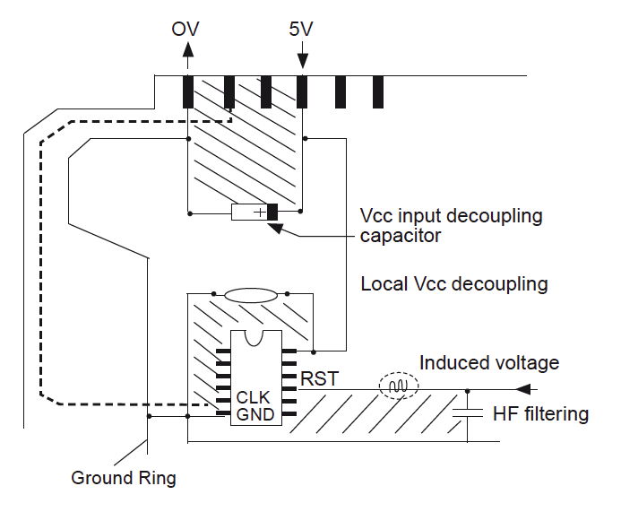
2.3 Signal Ground vs Chassis ground
Wether or not the PCB 0-V reference should be grounded to the equipment chassis and where is a recurring issue. EMC-wise, it is generally better to make the signal Gnd equipotential with the chassis, especially in the PCB area. Yet some designers, for preventing low frequency ground loops, keep the PCB isolated from the chassis ground. Considering the frequency domain covered by an ESD, this issue is irrelevant since even a floated PCB become virtually grounded above few tens of MHz anyway. If a PCB ground has to be floating, a VHF connection to chassis must be established, via a few nF ceramic capacitor, preferably in the I/O connector area.
2.4 PCB hardening with plastic products
An increasing number of equipments are designed with plastic housing, with no intention to apply a conductive coating. In such case, if all but one of the EMC constraints can be met with a non-conductive envelope, it would be a waste to change for a full metallized plastic just because of the ESD requirement. As a result, the PCB itself becomes the only physical barrier to ESD coupling. Even if only Indirect ESD is anticipated, a bare PCB and its active circuitry are first class targets for field induction. Here, all that have been said before has to be emphasized, especially regarding E-field, capacitive coupling. A PCB with at least a full ground plane on one side and a ground ring on the edge is a must. Since practically all complex ICs (μPs, ASICs, Flash memories, DSPs etc … ) have multilayered chip structures, the chip’s internal reference plane is tied to the PCB’s Gnd plane by the many Gnd pins of the IC package, such as the whole PCB plus IC assembly benefits from a monolithic ground plane.
Summary of ESD protection measures at PCB level
- Select ICs which are inherently ESD protected to ≥ 2kV ( HBM test).
- Clamp/ decouple critical inputs and Vcc pins, close to the critical ICs.
- Select logic technologies with longer risetimes, compatible with the function.
- Use PCB with ground (0volt) plane, w/o slots. Multilayers are best. If single layer/single side have to be used, landfill (do not etch) voids, with copper linked to all 0-volt nodes.
- No critical traces ( Clock, RST etc … ) near the board edges.
- Keep space for I/O ports decoupling with SMT components, right at entry points.
- All general EMC rules have a positive effect on ESD immunity, provided that the high frequency spectrum ( >300MHz) is kept in mind.
3. ESD protection by internal wiring an mechanical packaging
Several practices in component selection, placement, mounting, bonding and cabling can upgrade an equipment defenses against ESD. Two things are to consider for their selection: some components or subassemblies can be generators of internal ESD, some others can be carriers or even victims. In the ESD sources category are the parts made of insulating material that can be momentarily or permanently rubbing, rotating sliding etc … for instance :
– paper trays or containers
– plastic pulleys or rollers with rubber belts or conveyors
– cooling fans with polycarbonate blades
– High Voltage dc power supplies.
When such elements are selected, preference should be given to those which the manufacturer has made antistatic or static-free, through material selection, conductive additives or shielding. All metal parts around these items should be grounded to the metallic mainframe. High voltage dc supplies, due to the non-null value of their static field, can charge by influence all insulated parts (even metallic parts if ungrounded) that are in the path of the electric field lines. Such high-voltage dc sources should be surrounded by a grounded Faraday shield, neutralizing their stray capacitance vs. nearby components. In extreme cases of serious internal static generation, active static eliminators can be installed that ionize the air, allowing the separated opposite charges to recombine.
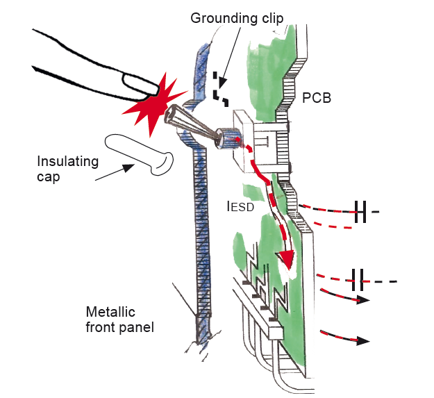
ESD protection of keyboards and flat displays
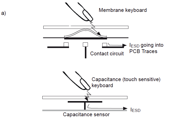
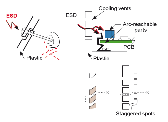
The other category of components i.e. the ”carriers” or ”victims” is by far the largest. A special problem is posed by the keyboards and specially the membrane type. First, these devices need an opening in the shield, creating a privileged entry port for ESD coupling. Moreover, they have a high chances of being hit by a direct discharge, whose arc directly reaches the touch-sensing circuits under the domes or capacitive arrays (Fig. 5). One need to know what sort of unwanted response to such discharge is acceptable or not. The criteria could be as liberal as “no-damage” only, or more demanding in cases where an illegal keyboard action could cause a dangerous reaction from the equipment. Several solutions exist for keyboards immunity, if the ESD risk is moderate:
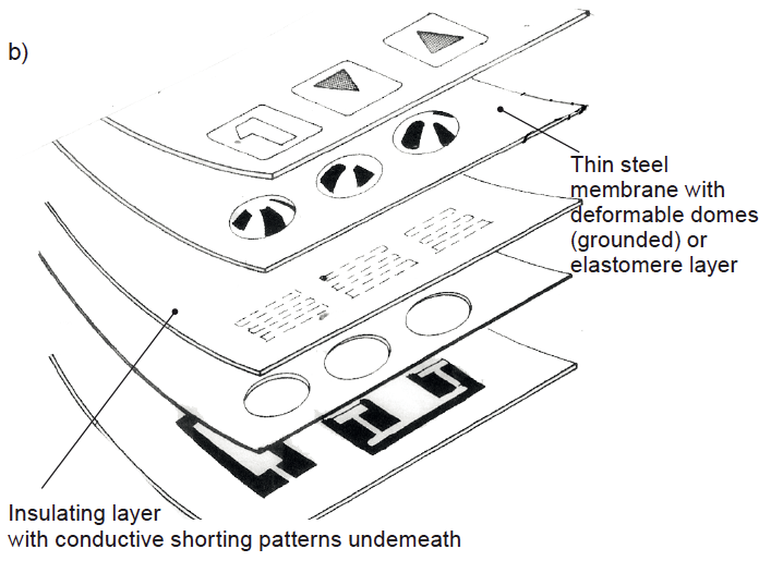
- Thin metal interlayer, multipoint grounded to the chassis so that the ESD current does not penetrate the inner part of the keyboard. Cheap versions exist where the flexible contact layer has simply a grid of conductive ink.
- For the outer membrane where symbols are printed, use a thick (0.3mm) polyester film which can resist to arc punch-through, and keep signal traces of the underlayer far from the edges to avoid a lateral flashing.
- Add 10 kΩ series resistors on the signal traces coming from the membrane, before the active circuits.
Contactless “virtual switches” keyboards using capacitive detection are naturally protected against ESD because their glass or thick dielectric touch panel can stand 15kV without breakdown. However the dielectric panel is sometimes porous, allowing cascades of internal arcing to reach the internal circuitry. Also, the capacitive current through the dielectric can exceed the detection treshold, causing an undesired switching. In both cases, 10kΩ series resistors, like for the membrane keyboard are a simple and efficient solution. TVS are not recommended because their significant parasitic capacitance could interfere with the capacitive sensor circuitry.
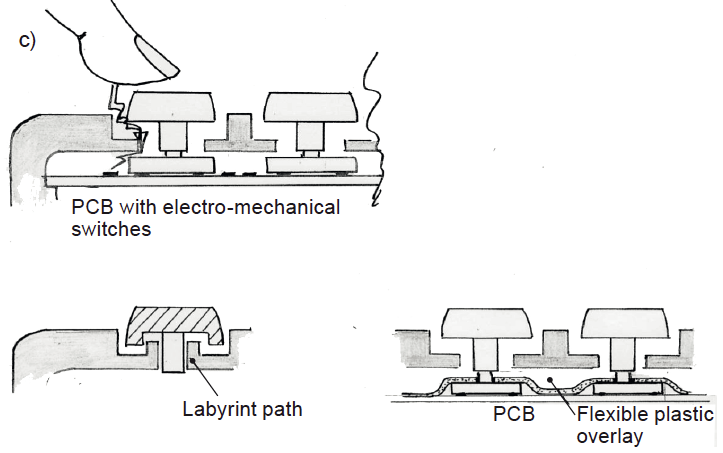
Regular button-and-pluger keyboards are not necessarily exempt from DESD intrusion, depending on the free air trip between finger tip and the PCB traces underneath. One solution consist in creating a labyrinth path for the key. An other solution is using a soft plastic overlay on the PCB, which can withstand up to15kV for the air discharge. This overlay is embossed above each switch, increasing the arc path length.
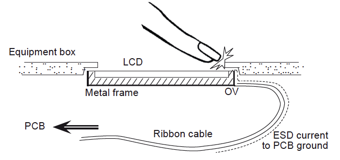
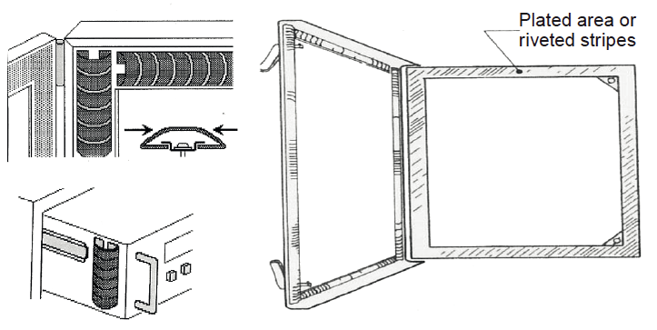
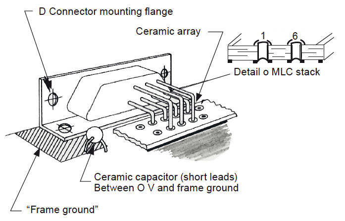
A similar problem occurs with LCD displays mounted flush on an equipment façade (Fig. 6). A discharge can reach the edge of the LCD frame, not necessarily fully evacuated by the housing. Making things worse, the LCD frame is often connected to an internal signal Gnd, such as the full discharge current can flow via the ribbon cable to the equipment boards. The solutions depend on the nature -conductive or not- of the housing:
With metallic (or conductive plastic) housing:
– a tight electrical bond on all sides, between the LCD rim and the aperture edge.
– a transparent, conductive overlay like ITO (Indium Tin Oxide), with a typical 3-10Ω/sq. Surface resistance, with edges bonded to the aperture stepped edge.
With a plastic housing, the display is treated as a sacrificed entry port for ESD: use a shielded flat cable, with the shield connected one end to the LCD frame, the other end to the PCB ground, or add 10kΩ series resistors on the signals coming out from the LCD, right at the cable entry on the main PCB.
Finally, ESD has to be considered in regard to the location of sensitive items like critical PCBs, magnetic sensors or storage media and their associated circuit etc … Not only their location should avoid the proximity of the ESD sources described above, but also the proximity of possible ESD entry paths like cooling or displays apertures, seams, openings etc … Near these places, shielding protection of the housing will be poor and ESD currents will re-radiate inside. If covers are bonded by straps, these straps will generate a strong H-field during a discharge. No sensitive components or their wiring should be placed close to them.
Internal wiring, exposed to ESD re-radiation inside, will also carry some induced ESD noise. Besides the precautions at their termination into the PCB connectors, the following guidelines will prevent excessive pick-up:
– Avoid long runs of cables along cover seams, hinges, bonding wires.
– Do not press cable harnesses and specially flat cables against the edges of metallic covers which are likely ESD targets : move them away from the edges, or use thick shield.
– Avoid large Vdc-to-Gnd and signal-to-Gnd loops. Always carry a signal close to its own return.
If, even after these precautions, an excessive ESD pick-up may still exist by coupling into Comm. Mode (cable-to-chassis) loops, use C.M. ferrite beads and sleeves over the whole cable. This solution will work best if the circuit is a low impedance one. Add-on ferrites exist in form of split beads and yokes. Some have been developped especially for flat cables and recent lossy ferrites materials can provide 6 to 15 dB of reduction above 30 MHz, which is precisely the domain where ESD couplings become critical.
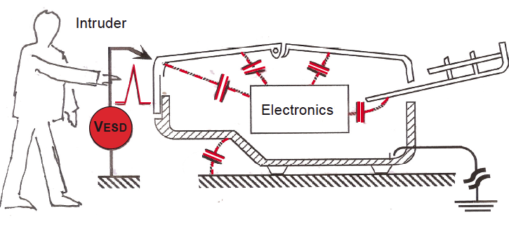
4. ESD protection by box shielding and envelope design
If the components, PCBs and internal elements have been hardened to a certain ESD level V1, while the specification requires a level V2 > V1, the housing is what is left to make-up for the difference. The shielding precautions for the housing are basically the same as for any EMI susceptibility problem, bearing in mind that the 300 MHz or higher spectrum of concern obliges the designer to consider the possible leakage of any seam and slot exceeding a few centimeters. This is not saying that a machine which relies on its housing for ESD hardening should be shielded with the same precautions as any VHF equipment or sensitive Radio Frequency device ! In the late 1960’s when ESD problems started to be a nightmare with computers, and its mechanisms were not understood yet, manufacturers of large computers were making all the covers RF-tight, entirely plating their frame with nickel etc … Main frames took-on the appearance a vault. Additional drawbacks are that the designer may not be familiar with these techniques which drastically increase the cost of the cabinet and associated hardware, complicate maintenance, accessibility, and may degrade with aging.
So, typically, we are looking for shielding methods which are economical, will remain unaltered after intensive use of the equipment, and provide a moderate shielding effectiveness in the range of 10 to 30dB (i.e. a reduction of electro magnetic field by a factor of 3 to 30 times). But they must provide this attenuation up to the 300-1000 MHz region.
4.1 Some Shielding Basics
Those readers not familiar with shielding basics are encouraged to read the Sept 2016 and March 2017 issues of EE magazine where EMI shielding principles and applications have been addressed. Here, we will focus on shielding applications that are more specific to ESD hardening.
Shielding effectiveness is defined as the ratio of the incident field to the residual field (the part that gets through).
For E (or H) fields: SE (dB) = 20 Log Ein / Eout (or Hin / Hout)
If shields were perfect, Eout, Hout, and therefore Pout would be zero. In practice, a shield behaves as an attenuator, performing on two cascaded mechanisms: Absorption which increases thickness, conductivity, permeability, frequency, and Reflection which increases with Surface conductivity and Wave impedance.
- The most threatening part of the ESD spectrum being in the high frequency region, any metal barrier with thickness of 0.1 millimeter or more, will provide an excellent absorption loss.
- Conductive paints or coatings will not perform well by absorption, because their film thickness represents only a few skin depths or less, hence a low absorption loss. Conductivity is the key: Silver, copper and zinc films would still provide some absorption loss in the range of what is aimed for ESD, i.e. 10 to 40 dB. Graphite paints, with relative conductivity of 10-5 to 10-6 will provide marginal or null absorption.
Regarding the ESD-related radiation, two situations may exist:
a) IESD: discharge does not occur on the conductive housing of the equipment itself, but rather it occurs nearby. In this case, the discussion on absorption and reflection applies. Furniture discharge will be most threatening because this is where H field predominates and the reflection term will be minimal.
b) The discharge occurs right on the housing (direct ESD). In this case the previous approach on near-field and reflection losses is irrelevant. What is impinging the metal barrier is not a field but already a current.
This current then penetrates the metal barrier, is attenuated, and what is left on the other side re-radiates inside. In any case, the only chance of a shield to perform well is to have either an excellent conductivity, as close as possible to copper, or a sufficient thickness to represent at least a few skin depths Yet, housings are not made like continuous metal cubes. Slots, seams, apertures etc … will inevitably leak. It is important to know its weak points, in order to establish some realistic objectives. In the high frequencies domain, where any solid metal would provide hundreds dB or shielding, these are never seen because seams and discontinuities fully spoil the metal barrier. ESD belongs to this case, so when chasing shields openings, one must remember that holes and seams are critical in areas that:
a) Are likely to receive an ESD, and
b) Have sensitive components or wiring just behind. An ESD-hardened box does not have to be a 120dB Faraday cage. A large slot should not be a designer’s hang-up if it is far from any critical circuit.
4.2 Maintaining Shield Integrity with Metal Housings
A metal housing already has the advantage of being a naturally efficient shielding barrier. All the efforts of the designer should be aimed at not spoiling this barrier with excessive leakages:
• All metal parts should be bonded together. Any floated item is a candidate for re-radiation : instead of being part of the continuous barrier, such piece may become a capacitive coupler to the electronics inside. Grounding of such part is not crucial; what counts is its equipotentiality with the other parts of the envelope (Fig. 7).
• For cover seams, slots, etc., how frequently they should be bonded is a design objective. A 10 cm leakage is worth about 15 dB of shielding against a 1ns pulse. If the goal is closer to 20 or 30 dB, seams or slots should be broken down to 5-3 cm. For permanent or semi-permanent closures, this means more screws or welding points or a conductive gasket. For covers, hatches, etc … it means flexible contacts or EMC gaskets. The often mentioned λ/10 rule implies that, for a 1ns rise time of the ESD, the distance between jumpers should be less than 0.1 m. Keeping such bonding intervals, and assuming that no sensitive circuits are located closer than 0.1m from this seam, a 15dB shielding can be expected. If more is needed, or if sensitive circuits are closer from the seam, distance between bonding straps should be reduced, which become rapidly unpractical.
• If bonding at the hinged side only leaves an excessive length of ungasketed seams, additional bonding points are necessary. In this case, use a few soft springs scattered along the cover edges. A variation of this shown in caption b) is using sections of spring contacts called finger-stocks. Several types are available, such as low-pressure, knife edge, and medium pressure. They require an adequate control of pressure by manufacturing tolerances, but they are extremely dependable. Grounding buttons or “sticky pads”, which are fairly compliant to gap variations thanks to their spring loading, can also by mounted simply by press-fit or self-threading stud.
• For a higher grade of shielding (20 to 40 dB), a continuous conductive bonding of seams is necessary, since a 30 dB attenuation at 300 MHz (λ/2 = 50cm) would require screws or rivets every 1.5cm ! Continuous conductive joints are available in several forms and stiffnesses (Fig. 8). The hollow conductive elastomer gasket is rather inexpensive to use because its elasticity compensates for large joint un-evenness and warpage. Here again, a good quality mating surface can be made by applying copper or aluminium tapes, which create a good conductive area for local shielding or contact points.
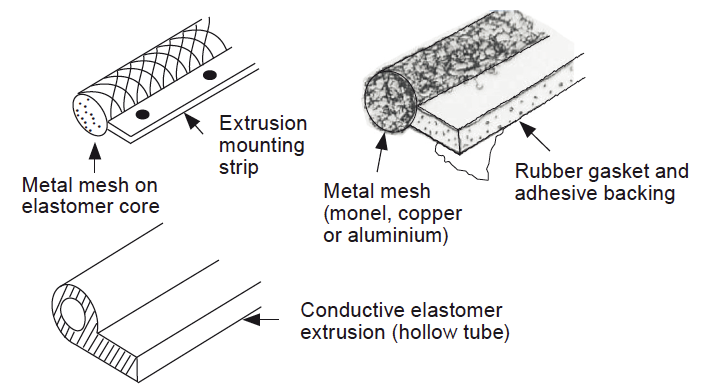
- Metal braid, mesh-type gaskets provide higher shielding, at the upper side of the required SE range.
- Finally, if even more hardening is necessary, the ultimate solution is shown in Fig. 9, the most efficient since 100% of the seam becomes a very good conductive joint. Besides its cost, it adds the need for a strong locking mechanism to ensure good, even pressure on all spring blades. This method is applicable to both rotating (hinged) or slide-mating surfaces. It is extremely rare that such extreme solution be needed just for ESD requirements. Independently of bonding, a reduction of the slot leakage can be obtained, at pratically no cost, by designing the cover edges so that they always offer a generous overlap. This acts by providing an attenuation known as waveguide-beyond-cutoff.
4.3 How to make shield barrier with plastic housings
Plastic housings provide no shielding whatsoever, so unless the PCBs and internal wiring can withstand by themselves the ESD threat (in that case, an IESD), the plastic must be made conductive. Several metallizing processes exist. As discussed before, conductive coatings exhibit a rather mediocre absorption loss, and they work mostly by reflection.
If a 30-40 dB SE range is desired, especially against low impedance sources like furniture/machine ESD, a conductive process with 1Ω / square or less must be selected. Another process, the particles-loaded plastic creates a volumic conductivity by inclusion of thin filaments or particles, providing absorption instead of reflection loss. Hovever the lack of surface conductivity complicates the bonding of metallic parts to the box skin, and it allows direct discharges, with multiple, cascaded arcing through the plastic barrier.
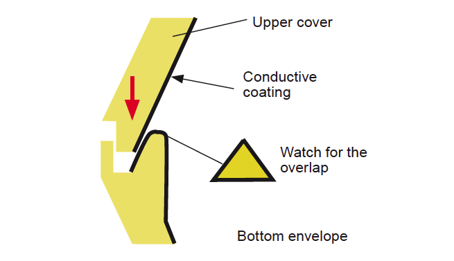
With a close look at the box design, some features of plastic housing can be turned into an advantage against ESD, and pitfalls can be avoided. For cosmetic and mechanical abrasion reasons, the conductive film is generally on the box inner side.This may also prevent any possibility of direct discharge, such as the equipment will be submitted essentially to IESD, while keeping the benefit of a shielded envelope. One exception is electroless or electroplating, for which the nickel or chrome plating is an aesthetic, hard surface that can be on the outer side. In this case, DESD will apply.
Some problems, though, are specific to metallized plastics:
a) If a conductive coating is relied upon to provide an overall shield, it must provide electrical continuity at the mating surfaces: top cover- to-base, side panels etc … With a plastic product, a continuous gasketing is sometimes expensive, so an alternative is to use tight tolerances for the mating faces, by designing a cross section that provides naturally a contact pressure (Fig 10). Make sure that the conductive coating extends:
– Deep enough over tongue-and-groove side to make a positive contact.
– But not beyond the groove center line, because this would permit direct ESD arcing in some areas that were not arc-reachable before.
b) Use a paint or coating having good adhesion and resistance to abrasion, for a reasonable number of closures and frictions of the mating edges.
c) If, thanks to its plastic enclosure, a product was declared as “class II” with respect to electrical safety categories (for inst. IEC Standard 435), one should verify that the metallization does not turn it into a “class I” isolation device. Except for these particular aspects, all that has been said for metal housings (slots, seams, bonding, etc.) applies to metallized plastic as well. Surface conductivity can also be improved locally by using copper tape.
4.4 Treatment of Shield Openings
Besides the joints and seams, several large holes may exist in the housing for Displays, Cooling, Cables penetrations, Fluid penetrations, Components shafts, etc… They create shield discontinuities with the same leaky properties as seams. In strict terms of EMI, they should be treated to provide SE performance equal to or better than the one required for the whole box. However, ESD bears some specifics. It is rather unlikely that people will discharge frequently near a display window or a cooling aperture. Yet, if the packaging is such that likely discharge points exist near these functional apertures and vulnerable circuits are located right behind , then apertures should be treated with wire mesh, conductive glass, etc… or a good sink path must be provided for the discharge current to flow on the box skin, not reaching the inner parts.
Toggle switches, LEDs and all indicator lights are another breech in the housing. Although feasible in sophisticated military equipment for instance, shielding a LED or small light bulb is cumbersome. A simpler approach consist in merely increase the breakdown voltage by adding an insulating, transparent lens which can resist to 15kV or more, depending on the ESD constraints (Fig. 11). Cables penetrations will be addressed in forthcoming Sect. 5.5, since the cable shield (if any) termination at the housing entry is a key factor in ESD immunity.
4.5 Non-Metallized Plastic Boxes
Conductive plastics, that is merely turning a plastic skin into a conductive one, can be treated it like a metal enclosure. However, an electronic equipment does not necessary have to be put in a conductive shell to resist ESD. Carefully designed PCBs and well decoupled I/O ports can allow a product to function trouble-free under all but the highest ESD threats, like IEC severity levels 1, 2 and 3. The key to the success, in this case is to make sure that only IESD can happen, and no direct arcing can reach a critical part inside. This implies:
- Using exclusively discharge-proof, non conductive shafts, toggles, indicators etc … with a sufficient dielectric strength to resist against a D-ESD.
- Keeping away from the openings (cooling, seams, assembly joints etc..) any active component, bare wire/trace or internal metallic part that could be reached by arc. This applies to obvious parts like magnetic or laser heads, discrete transistors or ICs metal cans, etc… but also to passive elements like internal brackets, screws and the like. Use a minimum 1mm/kV as a clearance rule. The creeping capability of an ESD arc is amazing, and even reasonably tight abutting joints can still allow an arc sneaking inside the box. If such clearance is impossible to insure for the highest ESD voltages, use a labyrinth design for the openings (Fig. 12).
Summary of ESD Protection Measures at Mechanical Packaging & Box level
- For metal housings:
– Bond together every metal part (floating items are candidates for re-radiation)
– Avoid long seams and slots: a 10cm empty seam is leaky at upper frequencies of ESD. Break them into smaller slots, or use conductive gaskets and waveguide beyond cut-off effect.
- For plastic housings:
– apply conductive coating with ≤ 1Ω/sq surface resistance, then treat like a metal housing.
– avoid long screws protruding inside.
– try to take advantage of air-gap and plastic thickness ( works for you at no cost)
- Respect shield integrity at cable entry points
- Parts location inside:
– locate more sensitive subassemblies and wiring deep inside, far from housing surface and openings
– locate less sensitive elements outboard from the above, acting as passive barriers
5. ESD protection of external cables an I/O ports
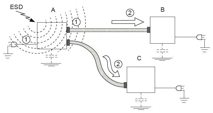
External cabling are a greater problem. Due to their direct illumination during ESD, they become unintentional, but efficient antennas, converting the radiated field into induced voltages and currents. Fig. 13 shows what is happening to external cables during an ESD event. To combat the effects of this coupling, two approaches are available, which depend on the nature of the external cables and of the equipment enclosure. If the external cables are shielded (maybe for other EMC reasons, and probably not just against ESD), they will perform efficiently against ESD, provided some precautions are taken, the same as those used for good RF shielding results. If the system external cables are not normally planned to be shielded, and the equipment box is eventually plastic, there is no sense in shielding them for meeting an ESD immunity level. In this case, the ESD-induced pulses could penetrate the equipment by the external cables conductors, and they must be filtered, or eventually clamped, at the cable entry port.
5.1 External Cables Shielding
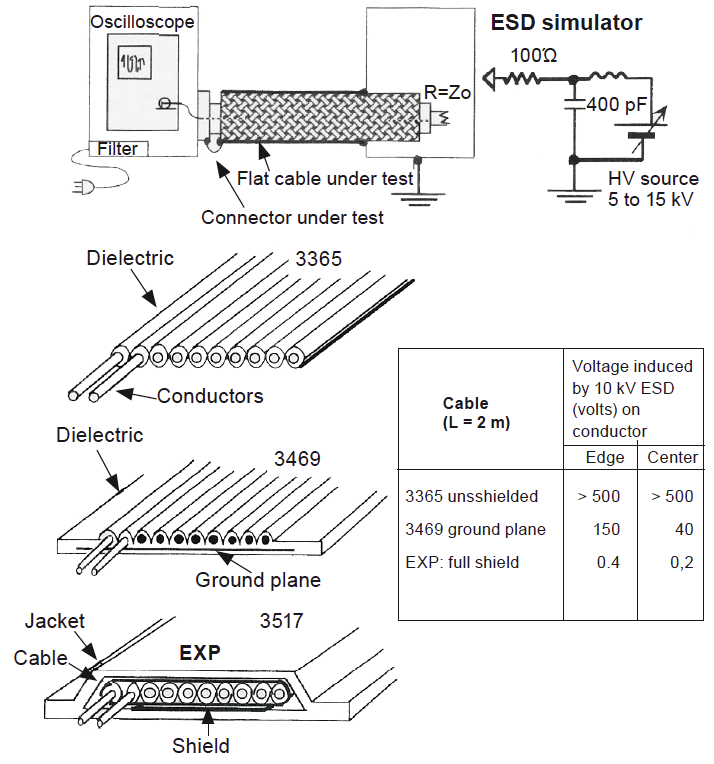
Although all cables are potential ESD coupling vectors, flat-cables come on top of the list because they are generally untwisted, unshielded and terminate on plastic connectors right on PCB inputs. They also offer a larger, more even stray capacitance to ground than multipair cables for instance, where wire pairs are convoluting randomly into the bundle. In a well documented set of experiments, C.Palmgreen (Ref. 6) has measured the voltage induced in flat cables by an ESD applied to the box where these cables were connected. From these tests, it is clear that for best ESD immunity, sensitive signals should use the central conductors of a shielded flat cable. Care should be taken to minimize the shield resistance by a) using cables with highly conductive shields; and b) providing low resistance, 360º shield contact to equipment frame. Unshielded and ground-plane cables provide no or little ESD protection.
With ESD, the empirical recipes about cable shields (”thou will ground the shield at one end only to avoid ground loops …”), which can be justified at audio or low frequencies, are irrelevant. To reduce ESD pick-up, a cable shield must be bonded to each housing that it penetrates. The argument that a floated shield will not allow the ESD current to flow and, therefore, will avoid coupling, does not stand a thorough analysis, nor the practical experience. The shield floated end reaches several hundred volts of CM voltage and will re-inject some of it by capacitive couping onto the inner wiring. One useful figure of merit is the shield transfer impedance, Zt. If a cable exposed to ESD is of the coaxial type, the noise appears due to the ESD-induced current coupling via the transfer impedance of the braid. (Details in Article; Electronic Environment 2.2016).
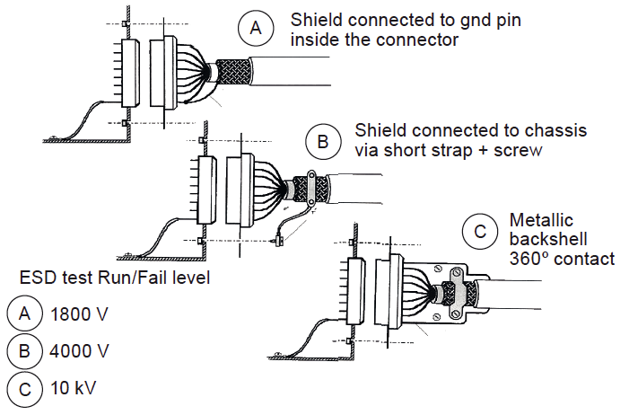
Since it provides the transition between the cable shield and the machine envelope, the bonding of cable shield to machine frame interacts with the box shield integrity addressed in former section. A most direct bonding of the cable shield to the outer skin of the equipment box will prevent the ESD currents carried by the shield from re-radiating inside. An example of this is seen on Fig. 15 with the drastic improvement when a good shield-to-box metallic contact is achieved.
Ferrites toroids, “the poor man’s shield”.
A ferrite toroid over an external cable cannot match the the 40-60dB attenuation of a real, good braided cable shield. However, although this bulge on the cable looks more as a desperate last minute fix, it provides 6 to 12dB reduction of the ESD coupling to the cable, which may be enough in some cases, for a solution that is inexpensive and easy to add on an existing cable without any hardware change.
5.2 ESD hardening of I/O Ports
In many applications, external cables are unshielded, and must remain so. Therefore, wether the box is metallic or not, the penetration of ESD-contamined wires inside the equipment is a serious threat, which must be controlled at the point of entry. This dictates that filters or transient voltage suppressors (TVS) be placed at the connector receptacle itself, or the nearest PCB area. When an I/O port receives unshielded cables, two cases have to be considered:
- No direct discharge (contact or arc) can access the terminals pins, or screws etc… Therefore only induced pulses, whose duration does not exceed few ns can penetrate the equipment. A filter with a good attenuation above ≈ 30MHz is generally sufficient.
- The terminals are exposed to both induction coupling as above, plus incidental direct ESD, where the full ESD pulse could be injected into I/0 circuits. In this case, filtering is needed for error-free response to the short pulses, and TVS are a must for a no-damage criteria because of the longer pulse (50-100ns).
A) Filtering short ESD induced pulses
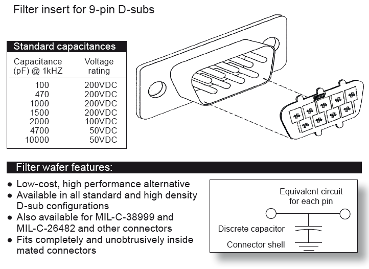
Simplest filtering is made by low value ceramic capacitors, preferably leadless (SMT) type. If leaded, they must be trimmed to the shortest possible length (Fig. 16). A 800pF disk capacitor with just 2 x 2 mm lead length starts loosing its efficiency at 100MHz, to become useless above 300MHz. Filtered connectors for through-panel or PCB mounting are very efficient above few tens of MHz, that is the bulk of ESD frequency spectrum. For the expensive types, each pin is constructed as a “Pi” or “T’ filter, giving a substantial attenuation in the VHF range (30 -300MHz). Cheaper models use miniature SMT capacitors mounted in the receptacle. They exist for most usual connector styles (Sub-D, Micro-D, USB, IEEE-1394, Ethernet/ RJ45 etc … ).
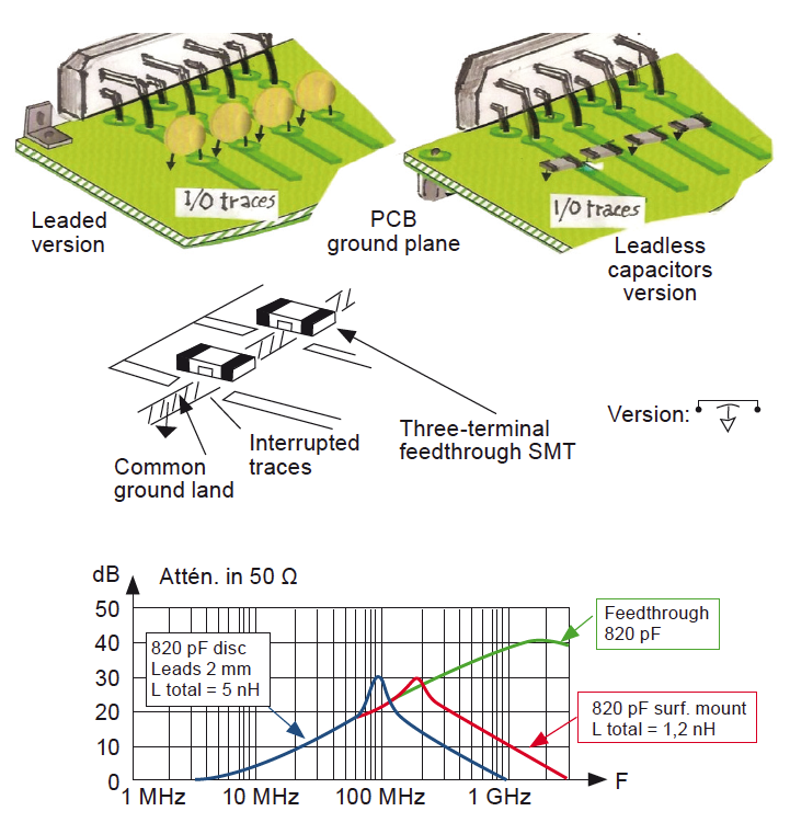
For PCB mounting, if the size, weight or cost of filtered connectors are prohibitive, economical substitutes can be made with surface-mount capacitors or planar arrays, close from the connector footprint (Fig. 17). Each incoming trace is decoupled to the PCB 0v Ref., or better to a chassis-connected copper land, with maximum precautions to avoid parasitic inductances. However, this is only a one-pole (20dB per decade) attenuation, so if the cut-off frequency requirement imposed by the I/O signal bandwidth is too high, say 100 MHz for instance, it will provide barely a 3 times (10dB) reduction at 300MHz. This may not be enough for an error-free objective against a 10 to 100V induced ESD spike.
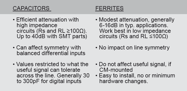
The amount of capacitance must be compatible with the bandwidth necessary for the useful signal carried on each line. These capacitors will be preferrably mounted in a common-mode arrangement, decoupling each trace to chassis ground. With differential or isolated inputs, if a capacitor C is decoupling each line to chassis, the incoming differential pair will see a capacitance C/2 .To get the full benefit from these decoupling devices, follow these simple rules:
- Compute the maximum capacitance tolerable w/o signal distorsion.
- Connect all the ground terminals of the capacitors (or arrays) to a copper land surrounding the connector area. Even with PCB 0V-ref grounded to chassis, this land should be preferably distinct from the 0volt plane, and directly connected to the nearest chassis point. As result, the ESD currents diverted by the filter will sink to the frame ground with minimum disturbance on the board.
- Keep these capacitors tolerances tight if they are used on true differential lines. This prevent the risk of C.M. conversion by capacitive unbalance, not only for ESD but for all RF emission /immunity aspects.
- Check for the surge voltage withstanding capability of the capacitors. In some environments, they must survive kV surges like for the Class-Y capacitors used in AC mains filters. This is especially true with isolated inputs, or PCBs with floating signal reference.
- Make sure that all I/O lines have been decoupled in the same zone. One single line (even a dormant one) left unfiltered can couple with the others.
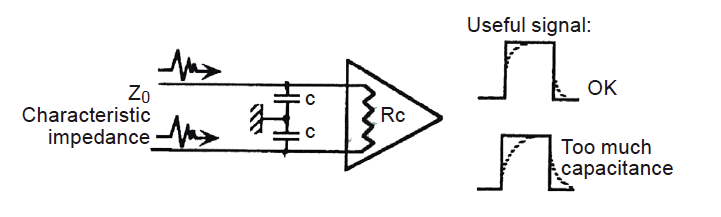
For computing the maximum value of tolerable capacitive filtering, Fig. 18. shows that, to avoid degrading a useful signal having a necessary bandwidth F max, we must keep:
2.Xc >> RT
With Xc = impedance of one capacitor at frequency Fmax.
RT = total impedance of victim Rload//Rsource, or Rload // Z0 (charact. Impedance for a long line).
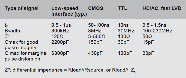
For a good pulse integrity (distorsion barely perceptibe), this condition is shown on Table 5.4, calculated for some typical digital data pulses.
Steeper attenuations are obtained at PCB level with inexpensive “T” filters made of 3-lead ceramic capacitors and small ferrite beads. Such components are available in leaded or surface-mount versions. The “100pF/100Ω” rule-of-thumb, often used by EMC practioners for standard EMI reduction above 30MHz, suits ESD as well. It means that a 100pF capacitor on the high impedance side, looking toward an analog or digital input, combined with a 100Ω series resistance (or a ferrite with≥ 100Ω impedance) will solve most RF immunity, emission and ESD problems. This results from the following, simple observation:
- No matter the actual load (victim’s side) impedance, provided it is ≥ 100Ω, and
- No matter the actual source (line side) impedance, A 100pF/100Ω team will always provide, at least, an attenuation of:
–10dB @ 50MHz, 20dB @ 150MHz, 30dB @ 500MHz (actually, 24dB Insertion Loss) For a single pulse, like ESD, this translate as a 10 times amplitude reduction (notice that the attenuation of a filter for an isolated pulse is less than that with a single frequency).
For last minute hardening, or when deep PCBs or hardware changes cannot be made, add-on parts can be used:
– The flexible insert filter of Fig.19 is manually fitted into an existing socket, turning an ordinary connector into a capacitive filter. Small tabs on the membrane edges allow a peripheral grounding to the metallic receptacle.
– Filtered Connector sockets exist for most standard connector types. The Male/Female filter adapter is a quick-fix version to be inserted between the two parts of an existing connector, without any hardware change. Like for the membrane-type, the existing receptacle should have a grounded, metallic shell.
B) Transient Voltage Suppressors against direct discharges on I/O terminals
Direct ESD can inject the full energy of a discharge into those circuits which are wired to accessible parts of the equipment. Such inputs, especially ICs, have a normal ESD immunity generally in the 2-4kV range (Re. Sect. 1, IC Protection). So, unless special ESD-hardened ICs have been selected, they must be protected by fast TVS.
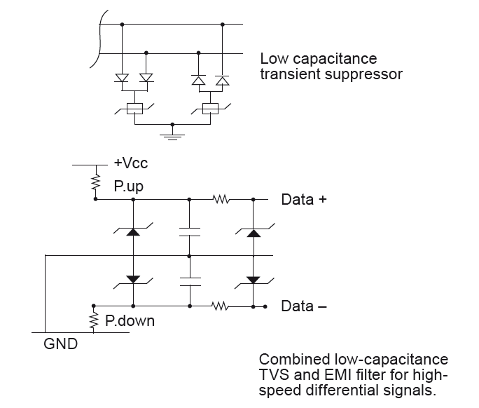
Varistors or Zener have significant intrinsic capacitance (typically few hundreds of pF) providing a filtering of the short pulses, at no additional cost. However, if the protected line is a high speed digital link or an RF input, this capacitance would bring too much distorsion. Special TVS modules are available with very low capacitance, like 5pF for High Speed Ethernet, or high definition video (Fig. 20). A few manufacturers have developed combinations of TVS + filter + single or balanced terminating resistors in a same integrated package, capable of protecting 2 to 10 lines. Other TVS ( by SMT or Littelfuse Inc.) are based on crowbar principle, where a thyristor is triggered, shorting the line to ground when its voltage exceeds the supply dc voltage. Flexible TVS membrane for connector sockets are available, for quick fix.
A cheap D-ESD protection can also be made with gas-tubes or airgaps. They are robust devices, but their firing accuracy and response time for a nsec. pulse front is mediocre, so they fit only for the less fragile applications. A rough overvoltage suppressor can be made by a 0.1 to 0.2 mm gap on PCB traces, firing approximately at 1- 2kV. Such devices should never be used on low impedance dc lines: the arc would not extinguish since it remains fed by the dc source.
C) Accessible pins of unused connectors
Depending on the equipment configuration and the type or number of interconnected units, some connector sockets could be left without cables. But if the inner wiring of the electronics is installed, these unemployed connectors are an invitation to serious ESD problem if they are accessible. A bare pin approached by a finger at less than 1 cm or so, can convey a direct ESD straight into sensitive components. Although some specifications are exempting these connectors from a contact or air-discharge test, it is recommended that such event be considered, at least as a no-damage criteria. Several solutions can be used:
- Do not install the inner wiring when the corresponding option is not present on this model.
- Mount the socket in a recessed area, so that a charged finger or handheld tool will zap the housing or connector edge first.
- Place a metal cap or blinder on un-used connectors.
- Place a plastic cap or blinder on un-used connectors, with a breakdown voltage > 20kV.
- Protect the corresponding lines with TVS ( not needed if the bare receptacle is not exposed).
- Use a simple mechanical shorting device, with a spring blade that grounds all the pins to the metallic receptacle rim when the connector is not there.
D) Opto-electronics as an ESD barrier
Opto-electronics often viewed as the panacea against EMI, would seem to be an ideal solution against ESD as well. Although they must not be rejected a-priori, they may give disappointing results:
- Optical Isolators (OI) have parasitic input-to-output capacitances that can represent 1 to 5pF, once mounted. For an ESD rise time in the nanosecond range, this is practically by-passing the isolation barrier by less than 1kΩ. Also, an OI can be activated by dV/dt ranging from 10V/μs for the cheaper parts to few kV/μs for the best ones. ESD transient reaching PCB traces easily exceed 10V/ns, triggering most OI except the High Immunity ones.
- Fiber Optics (FO) are certainly a better solution. But the designer is not exempted from carefully shielding and/or decoupling the detector end of the FO link.
E) Preventing ESD back-door entry by the power cord
Power cords are often overlooked in their contribution to ESD coupling, because they connect to transformer or other bulky, robust components. However, as it penetrates the machine enclosure, a power cord may carry to the inside the transients induced by ESD. Here, the solution resides in filtering/decoupling the power cord right at its point of entry. Since power cords are filtered anyway, this seems superfluous; but most RFI filters are optimized to meet conducted specifications below 30 MHz and may be inefficient in the >100 MHz range of ESD. In this case, the filter can be improved by additional ferrites, or mounted in a way that preserve its input-to-output isolation. Another solution, not mutually exclusive, is to use a shielded power cord, that will both prevent ESD re-entry and improve the drain path to ground.
5.3 I/O Cable ESD hardening with plastic products
If a product has a total plastic enclosure, with no conductive treatment, and the designer is confident that he can still meet the other EMC requirements (Radiated Emission limits, etc … ) it would be regrettable to be forced to a metallization just for ESD. At least it is worth trying a design pass without it. So we are left with I/O cables which are either: Shielded, with no chassis for connecting the shield, or unshielded. For shielded cables, although an all-plastic box make their use questionable, several solutions exist (Fig. 21):
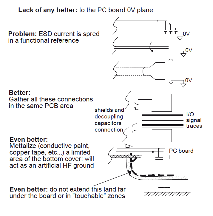
- Connect the shield(s) to the PCB 0Volt Reference. This is the less desireable option, because ESD currents drained by the shield will spread accross the signal reference.
- Connect the shield to an artificial ground (Fig. 21, bottom). This is a piece of metal foil or conductive coating, with at least a 50 cm2 area (with 100 cm2 being preferred), laid in the plastic housing, bottom side. Placed near the I/O entry points, this foil will collect the shield currents (instead of the 0V plane) and spread them to ground via the foil stray capacitance. Ideally, the cables shields should physically connect to this foil with a 360° joint. This is seldom practical, so the cable shields can be terminated on the PCB by a metallic connector housing, or clamp, then bonded to the artificial ground by a wide strap or bracket. The shield connection on the board should be a dedicated copper land, preferably not the 0V plane. With unshielded cables, the principle is to clean-up the wires of their ESD-induced noise before it contaminates the PCB. So HF decoupling will be used (see sect. 5.2, PCB), with the decoupling capacitors connected following the same rules as cable shields above:
- Connect the decoupling capacitors to the PCB 0Volt plane. This, too, is the less desirable option because it contaminates the signal reference (Fig. 21 top).
- Connect the capacitors to an artificial ground, made by a metal foil in the I/O ports area, not extending too far underneath the board (Fig. 21, bottom).
6. ESD immunity by software and noise inhibition techniques
ESD is generally an isolated, elusive event happening at worst no more than a few tens times a day, a few weeks per year. Therefore, software/firmware error detection and correction can be simpler and less expensive than adding components. The following few guidelines (some inspired by the excellent analysis of Ref. 8) can help to implement this “intelligent filtering”. However, one must remember that:
a) Nothing is free and the added instructions for “catch-all” error recovery increase the program size. Memory space can double, and execution time (cycles) can be multiplied by 1.5.
b) A lot of software traps are camouflages simply patching a more general vulnerability to all kinds of electromagnetic disturbances, not just ESD.
Non-damaging, low level ESD-induced pulses can cause severe errors and machine lock-up. Appearing on critical Processor/ Controller lines, like: Oscillator inputs, Reset, Interrupt Request, or also chip resident programming or manufacturing customization or debugger, they could corrupt or freeze a program execution. Several defensive software techniques, often embedded in the μProcessor itself, can be used:
- Software deglitchers (voting or polling techniques) to confirm the status of an input, using multiple reading.
- Error-detection methods like parity check, CRC check, HDLC, digital filtering, auto-correlation and … etc.
- Program run-away, detected by checking the time duration of routines, avoiding non-intentional executions.
- Regular, periodic programmed refresh, even without special aberration detection.
The I/O management connecting the processor to sensors, actuators or communication devices can periodically refresh the I/O port register to prevent any illicit change. For analog inputs, a regular check against a min/max range, based on history of a previous of values, will ignore an instantaneous value that is suddenly out-of range.
Many of these techniques are associated with dedicated safeguard circuit like the Watchdog, built-in the IC. The CPU generates a periodic signal as long as everything is okay. If not, a recovery is initiated (“deadman’s” detection technique). If the main program is stuck in a frozzen state, the watchdog will Reset/Restart the processor. This is often undetected by the user, hence tolerable. But in some cases, the reset is suspending the regular operation, becoming a nuisance. Or, if the Watchdog signal itself is triggered by an ESD, the scheme is defeated, and un-necessary restart will occur. For this reason, some test plans require that up to a certain ESD voltage, the EUT should make no error at all, even recoverable; reason being that such low voltage ESD occurences can be very frequent in some environments.
A leading idea for ESD hardening with firmware is mistrust: one should never assume that the state of an I/O port, register, memory address etc … has not changed since its last legitimate use. If an undesired change in the status of a line can trigger a wrong sequence, this line should be periodically refreshed, or checked / restored. This should be used only for serious cases, like when the sequence of events would end in a lockup, requiring operator action. Fault-tolerant architectures and “graceful recovery” require that the designer knows all kinds of output states that can legally exist. Concerning data lines in general:
- No circuit should be authorized to disable itself for an undefined period.
- Critical inputs, especially those which can trigger an irreversible sequence, should be checked twice.
- Make an “And” gating of critical signals with an undisturbed clock line. For instance, a RAM can be selfprotected against an illegal WRITE through an extended addressing; But if an ESD induces a same pulse on both the “Read/Write” and the “Enable” inputs, the protection is defeated.
Nevertheless, as said at the beginning, solving ESD problems by software tricks is basically “cheating”. Some other severe high frequency threats, like the exposure to strong RF fields (10V/m or more) and Electrical Fast transients with kV peak may exist which the software cannot handle. Their interference will be either quasi-continuous (with RF fields), or so recurrent (EFT means bursts of 50 pulses/sec) that autorecovery simply cannot work. The sofware will keep trying to restart a machine that is making errors over errors. Therefore, software defense has to remain the last barrier for rare, isolated events, not exonerating the designer to apply all hardware techniques described in this chapter.
7. ESD immunity with miniature, portable devices
An increasing number of small, hand-held or pocket-size devices are carried by a huge number of people. Just to name a few of these “nomads”, on a list which is extending every month: cellular phones and related accessories, palm-size personal agendas, low power wireless (Bluetooth etc …) devices like wireless mouses, USBs transceivers, USB keys, miniature FM radios, music players/recorders, RFID, some devices being body-implanted (cardiac peacemakers, hearing aids, insuline dispensers), smart car keys, GPS road maps etc … Regarding ESD, all of these share in common some remarkable features:
- They are light, plastic-encased, packed with complex electronics, often combining audio input/output, RF transceiver, hi-speed digital processing, optical sensors and image processing with small LCD or O-LED displays.
- Some incorporate one or more miniature RF antennas.
- They are constantly touched, carried or manipulated by people, therefore in nearest proximity of notorious ESD carriers: human skin and clothes, eventually car seats/upholstery.
- They often have accessible, subminiature I/O connectors.
So they appear as first class targets for severe I-ESD and D-ESD. Fortunately, several factors counterbalance these pessimistic expectations. Their size, generally no more than the palm of a hand and often less, result in very small exposed circuit loops and stray capacitance, with traces length not exceeding a few cm. Also, for obvious reasons, designers had to take serious precautions to preserve at once low RF emissions, high RF immunity and mutual compatibility of many internal functions packed into such small space. For instance, the PCB host for the active circuitry, generally a single miniature board, also acts as the supporting structure for integral or segmented shields, because the device’s plastic housing is just a physical shell without shielding. This PCB is a multilayer type, with the gnd plane frequently connected with ICs internal ground planes (see Sect. 2.3). The first layer (component face) has copper lands for soldering small metal covers with grounding tabs on the four sides.
The device plastic shells can be assembled together by a seamless process (ultrasonic welding, for inst.), such as the final casing is hermetic to arc discharge. Miniature connector sockets have a metallic housing grounded to the PCB, making it impossible to approach a charged finger without arcing on the metal edge first. For reducing the risk of a charged cable to discharge on sensitive pins at plug-in, these connectors can have a peripheral ground ring or sleeve that makes contact first. Miniature RF antennas are patch type which are not touchable. If a risk of air discharge remain at 15kV, miniature TVS with low parasitic capacitance and VSWR can be mounted on the antenna feeder trace. Same technique is applied to microphone inputs.
Thanks to these advantges and along with many other tricks, most of these nomad devices have a remarkable immunity. USB keys can resist to more than 10kV/m of RF field up to a GHz, with burst duration of 100ns, which is a more intense exposure than any closest ESD. Cellular phones do resist to the IEC 8kV contact and 15kV air discharges. Contactless car keys are generally damagefree (or code-erase free) up to 25kV, per ISO 10605.
8. ESD control at installation level
Installation environment is an aspect on which the designer has little control. Furthermore, since equipments are generally specified for certain environmental conditions, it would be foul-play to change the environment because an electronic device does not meet the challenge! Yet, life seldom provides clear situations like this. Many times the environment was not or poorly defined at the time of initial design, or salesmen might have overdone it and sold an equipment for an environment where it should not have been installed. So, if everything else fails or at least to provide temporary relief waiting for a more engineered solution, the following can be done:
- Maintain relative humidity above 50%, or use and ionized air blower.
- Install a grounded metallic rail, that everybody will touch when approaching the system.
- Use anti-static spray. Anti-static properties remain for about 2-4 months, depending on traffic. This does not bleed-off existing charges, but avoid static generation.
- Use seat pads in nearby chairs having breather-type fabrics.
- Ground the chairs (or carts) by using conductive wheels.
- Avoid carpet around system, use carpet with grounded woven metal thread, or cover the carpet with anti-static slightly conductive mats.
Floor conductivity has been a long-time concern in the electronics industry and industrial buildings in general. For instance, electrical resistance should meet NFPA Bulletin 56A issued by the US Natl Fire Protection Assoc. or, in Europe, DIN Std n°51953 & 53482 (Concentric electrode test). NFPA standard recommend a 25kΩ to1MΩ resistance of the installed floor, between two electrodes 1 meter apart. Another test often quoted is the “standard pedestrian”, where a person charged to 5kV walks lifting or shuffling his shoes on the specimen. Carpet is declared as conform if the residual voltage is < 2 kV within 2 seconds.
The parameters for anti-static flooring are:
a) Surface resistivity (Ω/sq.) relates to the propensity to static charging and retention. It does not necessarily mean that this carpet can “ground” an already charged person or furniture.
b) Transverse resistivity (Ω-cm) relates to volume resistivity i.e. the charge sink to ground.
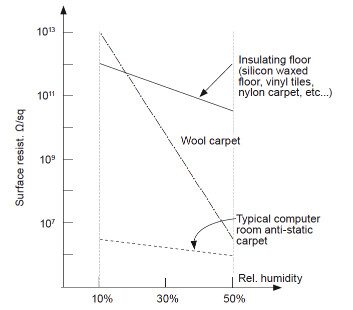
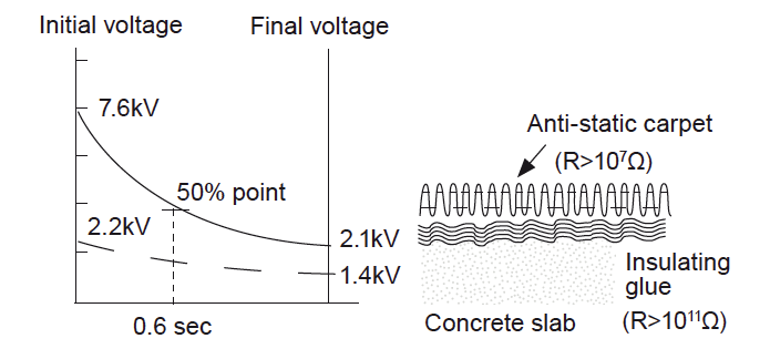
Anti-static floors must be installed properly, or treated later with certain cleaning impregnations. The anti-static carpet on Fig. 22 applied with a very insulating glue, may not generate static charges, per se, but cannot sink to ground the charges brought into the room by someone coming from outside. For this reason, anti-static (in fact static-disspative) carpets incorporating a % of metal or carbon fibers in the yarn should be electrically connected to the room earthing conductor. Floor tiles and desk overlays usin an internal carbon filler (Rs ≈ 105-107 Ω/sq.) should be grounded via a permanently contact to this layer.
Michel Mardiguian EMC Consultant, France m.mardiguian@orange.fr
REFERENCES & SHORT BIBLIOGRAPHY [1] Sicard,E, Bendhia, S, Baffreau, S, Ramdani, M.“EMC of Integrated Circuits” Springer, 2006. [2] Mardiguian, M. ESD, Understand, simulate and Fix, Wiley, IEEE Publ. 3rd edition, 2009. [3] Ming Dou,K. IEEE EMC Transactions , Feb.2008. [4] White, D.R.J., Mardiguian,M.“ Electromagnetic Shielding” Vol.3 EMC Handbook Series, 1988. [5] Ott, H. “Noise Reduction techniques in Electronic Systems” Wiley Interscience. [6] Palmgreen, C. “Shielded flat cables for EMI/ESD reduction”, IEEE/EMC Sympos., Boulder, 1981. [7] Boxleitner, W.”ESD and Electronic Equipment” IEEE Press. [8] King, M. “Mastering ESD System response”. EMC Technology Magazine, March & May 1988.