

The concept phase – EMI risk analysis . This article is a part of a series of texts that will deal with the EMC challenge in terms of project management and the practical EMC activities at different stages in the project flow.
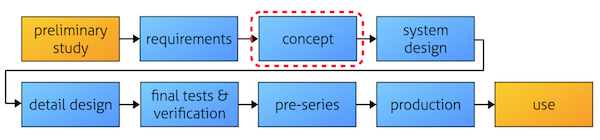
Different companies all have their own way of describing their project flow, so to keep it simple we will use the labels as given in Figure 1. We can call it a generic project flow. The picture only describes the basic outline of the work packages. These articles will describe the actual practical work we want to do in the project to “make EMC work” in a time- and cost-efficient way. Each part of our series will fill in the details for each part piece by piece.
We now reach the third block – EMI Risk Analysis in the concept phase–inour process picture, which is the one I found the most stimulating one. The design concept review – how is it going to work? What are the risks and what are our possibilities?
Here we find our brainstorm sessions, using the full spectrum of our imagination and our combined experience! This is where we set the stage for a successful EMC design, drawing the roadmap to follow for all involved. Too bad, EMI Risk Analysisis so often neglected – leaving you instead with the hectic troubleshooting activities; when it did not go that well in the EMC lab. You may find different articles about EMI risk handling, mostly related to complex installations. That type of work often results in evaluation charts and checklists for installations and component purchase. I will in this article show you some hints and examples on a smaller scale product level, focusing on the electromagnetic assessments and how to implement it in the physical design later on.
Why EMI risk analysis?
There is a widely spread myth that you must build a prototype before you start with EMC work for real. Possibly, that is related to that many engineers think of EMC work as a testing issue. But EMC work starts at square 1 in the project, and now we are already at stage 3. Now we know more about the EM environment and the requirements that we have set on the product. The design concept is now being settled, where we decide on how the functionality is to be achieved by means of different sub system hardware and software. By now, we have a basic idea of how many PCBs we are going to have, how long different cables are going to be and what type of signaling we are expecting. There is still quite some room for readjustment of the overall design concept, and since EMC involves the interaction between all parts and all EM active neighbor systems – this is the time for concise EMC work.
The content of the EMI risk analysis
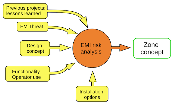
The EMI risk analysis – depicted in Figure 2 – is a critical activity that can provide much information at an early stage, where we address the issues;
- What are the electromagnetic neighbors
- How may coupling of disturbance occur?
- What must not happen?
- How do different installation scenarios influence?
- User interaction – what do they actually do with our product?
- Consequences of failure
- What did we learn in previous projects?
We will find possible ways of solution early, and several alternative solutions can be created and maintained in parallel. This provides more flexibility in project and reduces the need for late quick fixes.
An EMC design review can actually be regarded as an EMC test, where you are replacing the laboratory with an experienced EMC engineer. In comparison, what you get is;
- In the review you will find out what should be changed
- After a measurement, you just know that it does not work
- Short setup time for an examination
- Not dependent on functional subsystems or software
- Can be done at all stages of a design or installation project
- Can be effectively improved with EMC simulations
However, it does not give a result that can be directly checked against the requirement limits. Therefore, some physical EMC testing will be needed, such as measurements of EM fields. That is why you need to go to the EMC lab anyway; there are still too many unknowns to handle, but your risk of failure will have diminished greatly and you might even have a plan for redesign in advance.
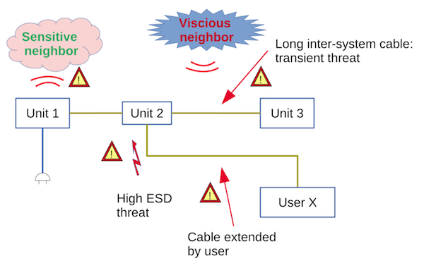
An example is shown in Figure 3, where we have a basic system with a set of sub-systems I call Unitsto make it very generic. These units can be PCBs, sub-racks, readymade devices or even buildings. When we look at these components from an EMC point of view, we ask questions on types of interfaces, length of cables, neighbor systems etc. This time, we find that there are certain risks with ESD generation when the user is working close to the display we are planning to have. We also discover, that some information from sensors etc will have to be retrieved at a long distance – increasing the risk of injecting high energy transients (surge etc) into the wiring. In addition, there will be some sensitive radio interfaces (IoT) in the vicinity. The other risks we have are more of ordinary level and are not listed here for simplicity. But: they shall not be forgotten in our complete EMC design.
In order to make the EMI risk analysis effective, you need a tight effectively working group that has the following competences:
- Application knowledge: what is happening in operating use
- System information: how is everything connected and communicating
- Hardware information: what type of electronics is being planned for (processor speed, types of signals etc)
- Software information: how resilient can we make the system in terms of optimizing the software
- EMC expertise with zoning experience
This means that this work is not just some activity that shall be “ticked off in a box”. You will need to plan dedicated sessions with experienced persons – and a very large whiteboard, because this is a very interactive live session. In our example, we have highlighted some specific risks that we specifically need to target with our design. The next step will be to set up our defense on a general level.
The zoning concept
To provide an EMC solution for the system we look at, we need to identify the protection measures needed – and where to put them. Zoning technology is an efficient tool for this work. We define electromagnetic volumes (zones) which we give unique identifications in the form of Z0, Z1and Z2. Between each zone, we have a zone boundary and that is where we want our attenuation to keep disturbances from spreading around. A zone can either be a noisy environment (that is contained to protect the surroundings) or a silent one (that has a barrier to protect the interior circuits). There are more technical details and rules to be followed, but I here focus on the process in itself.
The advantages with the use of a zoning concept are;
- It creates a roadmap for the EMC design
- The design choices are structured, and all involved may understand why they are made
- It creates a documentation that helps
- The interaction and dialogue between design groups
- Introduction of new designers in the project – especially useful when the designer who made the concept design leaves the project
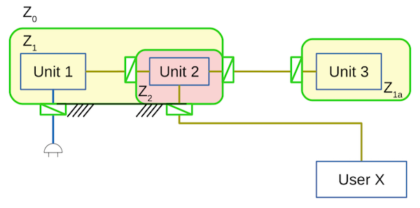
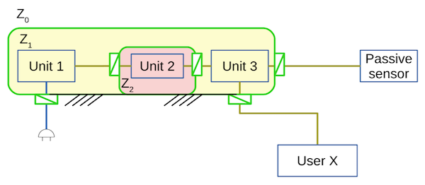
In figure 4, we have made the first attempt to solve the problem. This is solution number 1, where we identify our zones and barriers to match the risks. We place unit 1 and 2 in the same zone, since they will interact closely with each other. On top of that, we make an additional zone around unit 2, since it will be exposed to an increased ESD threat – and may also contain RF generating circuits that needs additional attenuation before entering into Z1. That means that we will have an additional interior barrier – at least for the time being. Later on, we might find that this concept is overkill, but we have identified the risk and keep it in mind. Unit 3 is placed far away, and here we need robust protection against transients at both ends of the signaling. And then we have the User Problem: the user is allowed to connect to their own equipment of undefined type. What will happen then? Better prepare for the worst: a robust barrier.
But we are not finished here. It is now essential to take a step back, take a break, contemplating the design and sleep on it overnight. Is there a better way?
We move on to another design solution. When discussing the matter, we find that the reason for the distance between Unit 2 and Unit 3 largely lie in the use of a passive sensor that needs to placed at a specific point. So we can split up Unit 3, having the sensor separate. We move Unit 3 into Z1, moving the transient threat from the communication to the sensor wires which might be easier (or cheaper) to protect. Moreover, we can shift the User interface from Unit 2 to Unit 3, making the design of Unit 2 simpler. So, we have created alternative 2 in Figure 5.
Which one is the best? Both are correct from an EMC point of view. That means that the choice depends on other aspects – product cost and user expectations etc. If we keep both concepts alive during the project, we can have a competition between the two solutions and maybe even have a Plan B if we strike severe problems during the remaining design phases.
Results from the analysis
The result we have for our example is an overview of the primary needs for the EMC design. We have a map to follow, for the rest of the project. Specific design risks are highlighted and listed for future design checks:
- ESD durability for the display design
- The transient protection filters: how much will they hold
- Ground structure for the interior of the zones – one combined in each zone to make shielding and filtering efficient
The other result is that we now have a short list of the primary EMC tests that we want to do in the early design phase:
- Radiated emission
- ESD at the display
- Transient testing (e.g. surge and burst) at the interfaces with long cables. For solution 1: three test interfaces. For solution 2: two interfaces.
Document structure
Where is the map?
We might regard the zone map in the same way as an orienteering map, which we use when we are walking/running in the forest. Now, imagine that a person is taking part in an orienteering competition. He gets a map and a compass at the start. Then he looks at the map for a while, and he throws the map away and races straight into the forest.
Would you expect that person to win the race? I wouldn´t…Yet, I have found myself looking at the same situation in many design projects. We make a very nice zoning analysis, take a picture of the whiteboard result – and then rush on with the design because there is not much time allocated. The photo is left somewhere deep in the digital storage system (in the folder Temp), getting obsolete over time. My part as an EMC advisor is revived again when the prototype is built – and it is time for testing.
So: keep a firm grip on the map, and take your time to look down on it during the design development. Do not throw it away. Rather, make sure to keep it updated and a live document that is actively used. That may call for a dedicated map reader – a person that helps the project manager to stay on a stable track in the EMI forest.
Input and output
As a summary, we find the following interface conditions to the other parts of the project flow.
Input from prestudy:
– Types of EM environments
– Expected customers – what do they do with the product?
– Differentiation on product configurations – what kind of installations should we prepare for
Output from this stage:
– EMI risk analysis
– EMC Zone design, first version (possibly multiple choices)
– First release of list of highlighted tests suitable for pre-compliance testing (e.g. listed in an updated version of the EMC compliance matrix)
– The first content of an EMC design check list (e.g. generated as an EMC design check matrix)
Closing remark
Many projects focus on high speed in the work, because you have your specific deadlines. It is then tempting to cut the corners in the beginning of the project and skip activities like the risk analysis – it is seemingly going faster. But risk analysis and zoning give you a steady pace in the correct direction. Early stage in-depth EMC analysis are therefore time saving – but only if you remember what you did, keep the information updated and available (= active registered document in the project).
Doing so, I am sure you will save much more money than you invested in this activity.
Lennart Hasselgren, Lic Eng. EMC Services, lennart.hasselgren@emcservices.se
If you have ideas and comments on this article, please feel free to mail me! Some might also recognize my short examples, and if you want to add something that would be an interesting talk.