

The Channel Operating Margin . (COM) is a figure of merit for a channel derived from a measurement or simulations of its scattering parameters. COM is a method to compliance check if a channel will work with a variety of different transmitters and receivers. The COM method reduces the overdesign that many other compliance check methods suffer from. The risk of overdesign increases with the speed of the link. The higher the speed is the higher is the risk of overdesign with added extra cost as result.
Introduction
In the design of high speed serial links it is important to verify that a channel will work with a bit error rate (BER) equal or lower than required. In many cases the transmitter and the receiver are unknown circuits. For example, a backplane link might live for 10 years or more.
In the design phase, of the backplane, the designer does not know what daughter cards will be used with the backplane 10 years from now. To design the backplane, to handle all possible existing and future coming transmitter and receiver circuits with required BER, is very difficult without support from a standard. Standards describe requirements on the channel to secure to work with varying types of existing and coming circuits. For example, specify IEEE 802.3 [1] the requirements for Ethernet, and OIF for the electrical part of an optical link [2].
Traditional methods for compliance check, with specified parameters in frequency domain, often gives an overdesign with added extra costs as result. With increasing speed the over design tends also to increase. With speeds of 25 Giga bit per second (Gbps) or higher the traditional method will reject many channels that in reality works. COM is a new method to compliance check a channel. COM reduce the over design and gives a rater secure check of the channel.
This paper will mainly focus on the compliance check of the channel between the transmitter and the receiver.
High speed serial link
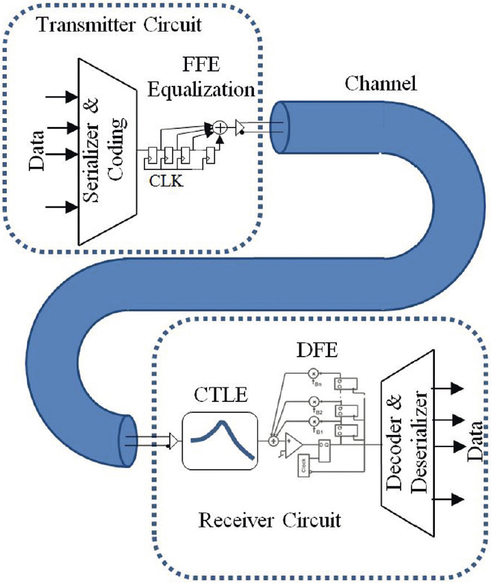
A high speed serial link consist of a transmitter circuit, a channel and a receiver circuit, see figure 1. The thru channel is normally specified from the transmitter circuit solder ball to the receiver circuit solder ball. To this thru channel is crosstalk channels added. The crosstalk channels are also normally specified from the aggressor transmitter circuit solder ball to the victim receiver circuit solder ball. Different types of equalizers are used to compensate for losses and reflections etc. in a channel.
In the transmitter a Feed Forward Equalizer (FFE) is normally placed. The FFE has a de-emphasis function. In the receiver a Continuous Time Linear Equalizer (CTLE) is normally placed. The CTLE is a peaking filter that gains the higher frequency spectra of the signal. Both FFE and CTLE will compensate for the attenuation of the signal caused by the losses in the channel. Losses increase with frequency and both FFE and CTLE gain up the high frequency spectra. A Decision Feedback Equalizer (DFE) is normally place in the receiver.
DFE is a nonlinear equalizer mainly handling inter symbol interference originating from, for example, dispersion caused by losses in the channel, and reflections. Equalizers cannot handle crosstalk noise but the signal to crosstalk noise ratio might be influenced by the equalizers settings.
Compliance check of high speed serial links
For example Ethernet specification [1] states that a protocol of the compliance check of the link must be written. This document is called ‘Protocol Implementation Compliance Statement’, PICS. The protocol consist of several sub parts as
- Implementation identification
- Protocol summary
- Major capabilities/options
- Functional specifications
- Transmitter characteristics
- Receiver characteristics
- Channel characteristics
- Environmental specifications
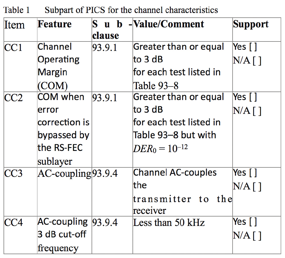
Table 1 below shows the part of the compliance statement in PICS for the channel of a 100GBASE-KR4 link, a 100G backplane link. Here is COM stated as the compliance check method.
Different compliance check methods
Compliance check can be done in different ways. Below are listed some methods.
A. Set up a link with existing hard-ware (HW), and measure the BER.
To setup a working link and check the BER require working HW. The major drawback with this method is that the HW is required and then the design and HW production must be finished before a compliance check can be performed. This will limit or eliminate the possibility the check for compliance in the design phase.
The compliance check will be performed very late in the design process. Also, only the today existing circuits can be used in the check. Future coming circuits cannot be checked as they do not exist. And we normally do not know the performance of the transceivers used in the check. The circuits might be ‘5-star’1 circuits that can handle severe problems in the channel. In a future use, ‘1-star’ circuits might be used and the link might fail due to the poor channel.
B. Simulation with specific circuit model.
To make a simulation of a channel with models of real transmitters and receivers will give, if correct models are used, a good estimation of the BER in the link. Simulation could be performed with models as, for example, IBIS-AMI. This type of simulation can be done in the design phase of the channel and do not require HW to measure on. One drawback of this method is that simulation models exist only for today existing circuits. No verification can be done for future coming circuits.
Also, the quality of circuits, used in the simulation, might be a ‘5-star’ circuits that can handle severe problems in the channel and cause problems in future with the link, when other non ‘5-star’ circuits are used as discussed in section A of this chapter.
C. Compliance check with plots of characteristics.
The traditional compliance check of channels is to check if a plot of some characteristics of the channel is on the right side of a limit line. Such characteristics are for example, insertion loss (IL) and return loss (RL). Figure 2 shows example of how an IL and a RL are checked toward limit line.
1 A ’1-star’ circuit has the minimum required equalizer functionality and a poor package. A ‘5-star’ circuit has excellent equalizer functionality and an excellent package.
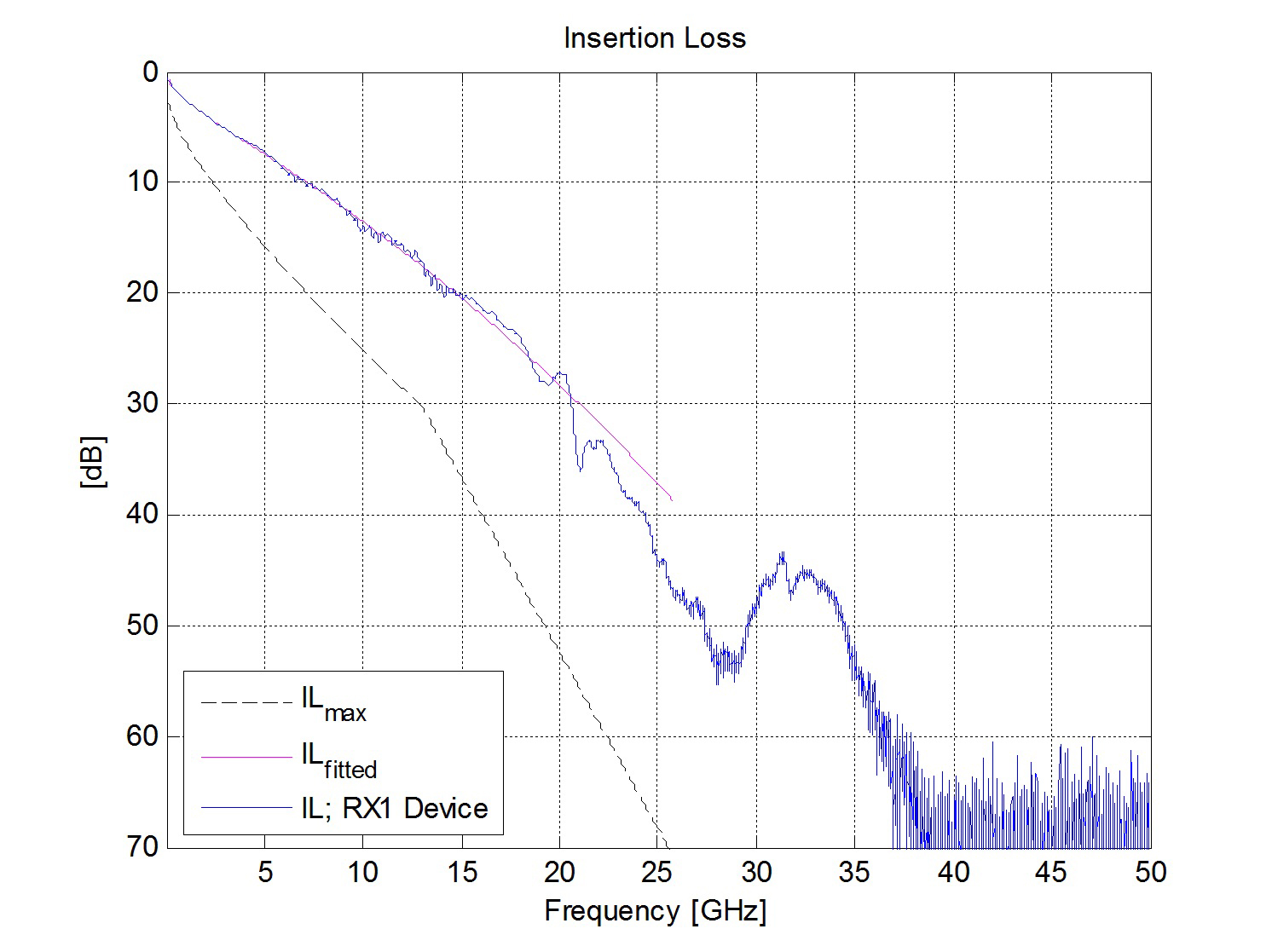
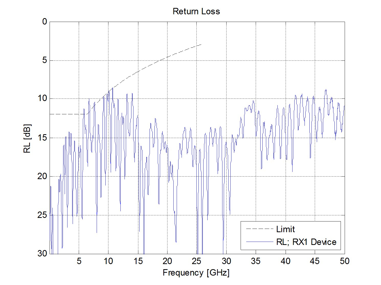
In the figures one can see that the IL shows large margin to limit line but RL pass slightly the limit line. Strictly, this channel will not pass the compliance check as the RL does not fulfill the requirements. But in practice, will the channel probably work as the large margin in IL will allow more RL. It is difficult to know the coupling between different characteristics in frequency domain and its influence on BER. It is then difficult to perform a ‘give and take’ approach between characteristics with large margin and characteristics with no margin.
A number of characteristics need to be checked. The higher the bit rate is the more characteristics need to be checked. The limit lines should be set to a level that, if all characteristics touch its limit line, the system should still work. If one characteristic pass the limit line the system might get a too high BER. But a channel with large margin to the limit line for one characteristic might be allowed to pass the limit line for another characteristic and still work fine. To have all requirements on the right side of the limit lines will generate an over design. A larger margin than required will be built in into the system.
D. Compliance check with COM
One coming method to compliance check of a channel is to use the COM method. The COM method is described in the next chapter. COM will reduce the over design and also secure, with high probability, to work with future coming circuits. COM is developed from StatEye and other similar statistical simulation tool for compliance check.
Compliance check with COM
COM is a simulation method with generic transmitters and receiver included together with the channel. The generic transmitters and receiver models are defined in the link standard. Produced transmitters and receivers must fulfill the minimum requirements of the standard.
A real circuit used in a link will then be equal or better than the model used in the COM compliance check. This gives a future proof verification of the channel as the future coming circuits is as good as or better than the model used in the compliance check.
The circuit models include the minimum required equalizers, filters etc. as specified in the standard. The simulation models also include a model of the package. All transmitter or receiver, placed on the market, needs to be checked if they fulfill the minimum requirements for the generic COM circuit. The procedure to verify a transmitter or a receiver is specified in, for example, the standard IEEE 802.3 [1]. If in practice a better circuit than the default specified in the standard is used the COM method will also result in an overdesign. But this overdesign will be smaller than the older traditional methods.
Function of COM
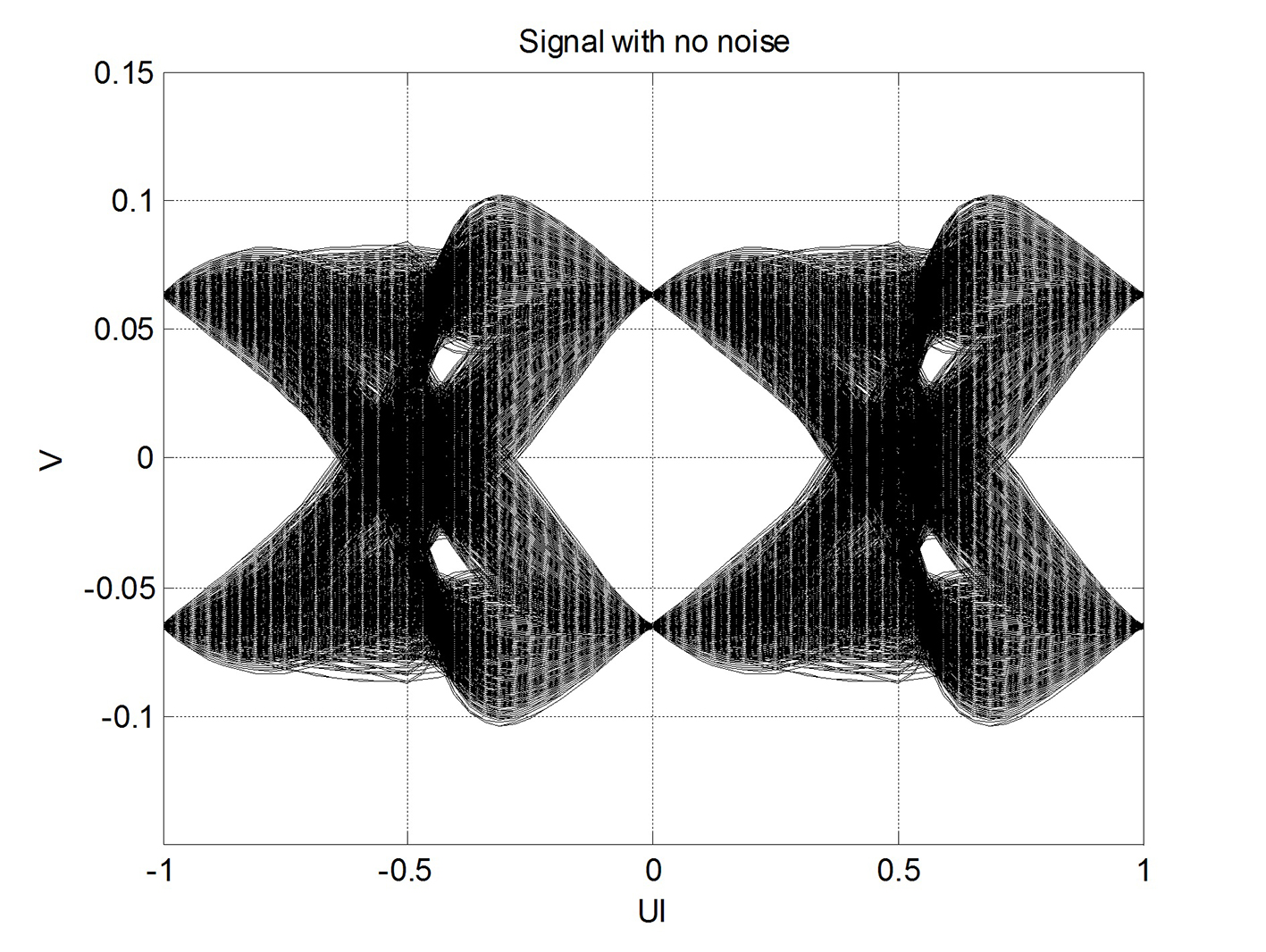
The COM procedure is specified, for example for Ethernet, in Annex 93A in IEEE 802.3 [1]. COM for Ethernet shall be calculated using the method described in this annex. COM is related to the ratio of a calculated signal amplitude to a calculated noise amplitude as defined by equation (1).
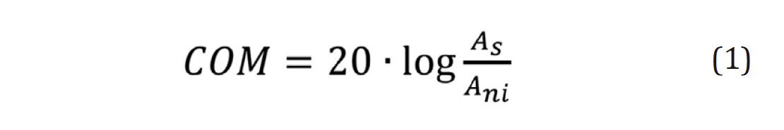
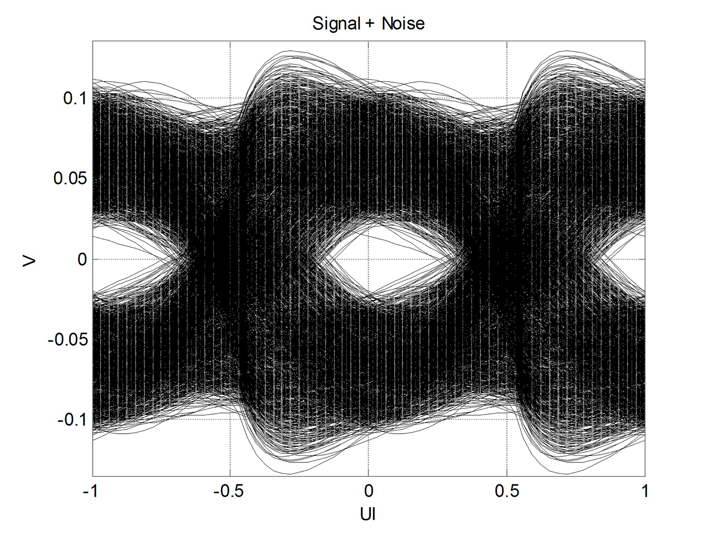
Where As is the amplitude of the sampled signal, at the receiver, after all equalizers see figure 3. Ani is the peak to peak amplitude of the noise at the sampling point given target detector error ratio for the channel (DER0) see figure 4. As the noise consists of random parts its peak to peak amplitude will increase with time. So Ani is calculated to be the noise level at given DER0. DER0 is the bit error rate at the sampler in the receiver. After the sampler a forward error correction block (FEC) can be used. If FEC is used the BER after FEC will be lower as several faulty bits can be corrected.
So several faults caused by the channel will be corrected in FEC and the link will see a much lower BER than DER0. For example a DER0 of 10-5 gives after FEC a BER = 10-12. But FEC introduce extra latency of the data to pass the link. Some applications cannot accept this extra latency and can then not use FEC. The COM value is, in one way, the signal to noise ratio given in dB.
The backplane channel and cable assembly for Ethernet states that, the COM value shall be greater than or equal to 3 dB for each COM test. This minimum value allocates margin for practical limitations on the receiver implementation as well as the largest step size allowed for transmitter equalizer coefficients. The compliance check is built on statistical calculations, simulations and other limitations. COM can then not guarantee that the channel will work with given BER for all configurations if margin is very low. But the probability to fail is rather small.
In the COM calculations it is assumed that the link, including transmitter and receiver (not including DFE), is a linear and time invariant system (LTI-system). Linear means that the signals are linear added on top of each other. Or more mathematically, the relationship between the input and the output of the system is a linear map. For example a crosstalk signal is linear added to the thru signal and then the receiver signal is the sum of the thru signal and all crosstalk signals. Time invariant means that whether we apply an input to the system now or T seconds from now, the output will be identical except for a time delay of the T seconds. The LTI-system allows calculation of the signal at the receiver as a pulse response. A summation of large number of pulses distributed in time gives the signal train.
Observe there is no compliance EYE-mask at the receiver sampling point in the calculation of the COM value. It is only the quota between signal and noise at the sampling point.
Procedure to calculate COM
The procedure to calculate COM is given in IEEE 802.3 Annex 93A. The channel must be described as a differential-mode scattering parameters, S-parameters. S-parameter models for the thru channel and all the crosstalk channels. Around this channel model is packages, equalizers etc. added. Parameters for the packages, equalizer characteristics, etc. for 100GBASE Ethernet are given in the standard IEEE 802.3.
COM reference model
Figure 6 below shows the COM reference model given in IEEE 802.3 Annex 93A.
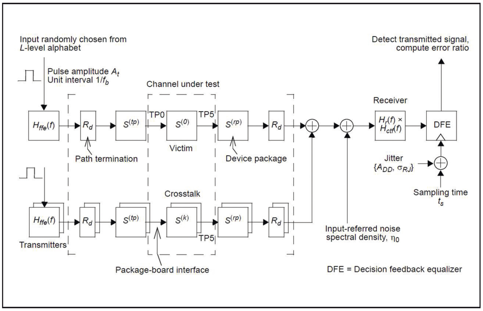
The pulse response, in time domain at the sampling point, is calculated after the DFE equalizer. The pulse is calculated with the optimal equalizer settings. The pulse value at the sampling point is set as As in the COM calculation. All valid equalizations settings for the FFE and CTLE are simulated in the search of the maximum As.
Noise probability density function (pdf) are calculated for each disturbance source. Noise as inter symbol interference (ISI), voltage noise, crosstalk, jitter etc. is considered in the calculation of the combined total noise pdf. The noise level, Ani, at the sampling point, for the specified DER0 is calculated from the total noise pdf. With estimated As and Ani can the COM value be calculated as given in equation (1) and checked toward the required margin.
Conclusions
In the design of high speed serial channels, with a flexible use of varying transceivers, both existing and future coming, it is important to secure that all combinations of used circuits will work. Traditional compliance check methods as, for example, plots of characteristics and limit lines, gives in many cases an overdesign with increase of cost or functional limitations as results. The overdesign tends to increase with transmission data speed.
Compliance check with COM reduces the overdesign as it allows the ‘give and take’ approach between different channel characteristics. This reduction of overdesign makes the COM method attractive and starts to be spread to other standards than Ethernet. Especially to links with high speed. Examples of links using COM are CAUI-4-C2C (also specified in IEEE 802.3) and the new coming JEDEC JESD 204C.
Ingvar Karlsson Ericsson AB, Kista, Sweden
References
[1] IEEE Standard for Ethernet, IEEE 802.3.
[2] Common Electrical I/O (CEI) – Electrical and Jitter Interoperability
agreements for 6G+ bps, 11G+ bps and 25G+ bps I/O,
OIF-CEI-03.1.
[3] Richard Mellitz, Intel, Various Topics for Computing Channel
Operating Margin (COM). 2014.
[4] Matthew Brown et.al. The state of IEEE 802.3bj 100 Gb/s Backplane
Ethernet, DesignCon 2014.